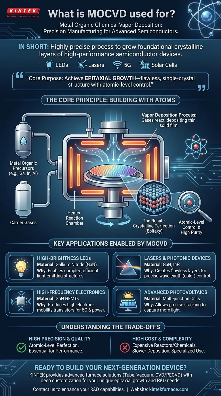
In short, Metal Organic Chemical Vapor Deposition (MOCVD) is a highly precise manufacturing process used to grow the foundational crystalline layers of high-performance semiconductor devices. It is the essential technology behind modern LEDs, lasers, 5G amplifiers, and high-efficiency solar cells. MOCVD operates by depositing atoms in ultra-thin, perfectly ordered layers onto a wafer to build up complex electronic structures from the ground up.
The core purpose of MOCVD is not just to deposit a thin film, but to achieve epitaxial growth—creating a flawless, single-crystal structure with atomic-level control. This perfection is what enables the unique electronic and optical properties required by the most advanced semiconductor components.
The Core Principle: Building with Atoms
MOCVD is a specialized form of Chemical Vapor Deposition (CVD). Understanding its components helps clarify its unique role.
The "Vapor Deposition" Process
At its heart, the process involves introducing precursor gases into a reaction chamber containing a substrate, typically a wafer made of sapphire, silicon, or silicon carbide.
The chamber is heated, causing the gases to react and "deposit" a thin, solid film of material onto the wafer's surface, one atomic layer at a time.
The "Metal Organic" Precursors
The term "metal organic" refers to the specific precursor gases used. These are complex molecules that contain the desired metal atoms (like gallium, indium, or aluminum) bound to organic compounds.
Using these specific chemical precursors allows for exceptionally high purity and precise control over the composition of the final deposited layer.
The Result: Crystalline Perfection
The goal of MOCVD is to create a film that perfectly mimics the underlying crystal structure of the wafer. This process, known as epitaxy, results in a large-scale, defect-free crystal.
This structural perfection is non-negotiable for high-performance devices, as even minor defects in the crystal lattice can ruin its electronic or optical performance.
Key Applications Enabled by MOCVD
MOCVD's precision makes it indispensable for manufacturing devices where material quality directly dictates performance.
High-Brightness LEDs
Virtually all modern high-brightness LEDs (HB-LEDs)—including the blue LEDs that enable white light—are manufactured using MOCVD. The technology is used to build up the delicate multi-layered structure of gallium nitride (GaN) that efficiently converts electricity into light.
Lasers and Photonic Devices
Semiconductor lasers, which power everything from fiber optic communications to Blu-ray players and facial recognition sensors, rely on the flawless crystalline layers created by MOCVD. The precise thickness of each layer determines the exact wavelength (color) of the laser light.
High-Frequency Electronics
MOCVD is critical for fabricating high-electron-mobility transistors (HEMTs). These components, often made from GaN, are essential for high-frequency and high-power applications like 5G base stations, advanced radar systems, and efficient power converters.
Advanced Photovoltaics
The world's most efficient solar cells are multi-junction solar cells, which contain many different semiconductor layers stacked on top of one another. Each layer is tuned to capture a different part of the solar spectrum. MOCVD is the only practical way to produce these complex, high-performance stacks.
Understanding the Trade-offs
While powerful, MOCVD is a highly specialized tool used only when its precision is absolutely necessary.
High Cost and Complexity
MOCVD reactors are sophisticated, expensive machines. The metal organic precursor chemicals are also costly, and can be toxic and flammable, requiring significant safety infrastructure.
Slower Deposition Rates
Achieving atomic-level perfection is a slow, deliberate process. For applications requiring thick, less-critical films (like protective coatings), other faster and cheaper deposition methods are far more suitable.
Not for All Materials
MOCVD is the master of compound semiconductors like Gallium Nitride (GaN) and Indium Phosphide (InP). However, for depositing simpler films like silicon nitride insulators in standard microchips, other variants of CVD are more economical and efficient.
Making the Right Choice for Your Goal
The decision to use MOCVD is driven entirely by the need for crystalline perfection in the final device.
- If your primary focus is optoelectronics (LEDs, lasers): MOCVD is the non-negotiable industry standard for producing the core light-emitting or light-sensing structures.
- If your primary focus is high-power radio frequency (5G, radar): MOCVD is the key enabling technology for creating the advanced Gallium Nitride (GaN) transistors required for high performance.
- If your primary focus is general microchip fabrication: You will encounter other CVD methods more frequently for depositing insulating or protective layers, as MOCVD is a specialized tool for active device layers, not bulk films.
Ultimately, MOCVD is the atomic-scale construction technique that builds the engines of our modern photonic and wireless world.
Summary Table:
| Key Application | Material/Device | Why MOCVD is Essential |
|---|---|---|
| High-Brightness LEDs (HB-LEDs) | Gallium Nitride (GaN) | Enables epitaxial growth of complex, efficient light-emitting structures. |
| Semiconductor Lasers | GaN, Indium Phosphide (InP) | Creates flawless crystalline layers for precise wavelength control. |
| 5G & High-Frequency Electronics | GaN HEMTs | Produces the high-electron-mobility transistors needed for power and speed. |
| High-Efficiency Solar Cells | Multi-junction cells | Allows precise stacking of different semiconductor layers to capture more light. |
Ready to Build Your Next-Generation Semiconductor Device?
Leveraging exceptional R&D and in-house manufacturing, KINTEK provides diverse laboratories with advanced high-temperature furnace solutions crucial for processes like MOCVD. Our product line, including Tube Furnaces, Vacuum & Atmosphere Furnaces, and CVD/PECVD Systems, is complemented by our strong deep customization capability to precisely meet your unique epitaxial growth and materials research requirements.
Contact us today to discuss how our solutions can enhance your R&D and production capabilities.
Visual Guide
Related Products
- Multi Heating Zones CVD Tube Furnace Machine for Chemical Vapor Deposition Equipment
- 915MHz MPCVD Diamond Machine Microwave Plasma Chemical Vapor Deposition System Reactor
- Molybdenum Disilicide MoSi2 Thermal Heating Elements for Electric Furnace
- Multi Zone Laboratory Quartz Tube Furnace Tubular Furnace
- Molybdenum Vacuum Heat Treat Furnace
People Also Ask
- What is the function of a multi-zone tube furnace in CVD synthesis? Master 2D In2Se3 Nanosheet Precision
- What are the advantages of multi-zone tube furnaces? Achieve Superior Thermal Control for Advanced Materials Processing
- What role does a Tube Furnace play in the CVD growth of carbon nanotubes? Achieve High-Purity CNT Synthesis
- How are multi zone tube furnaces used in ceramics, metallurgy and glass research? Unlock Precise Thermal Control for Advanced Materials
- What are the main applications of multi zone tube furnaces in university laboratories? Unlock Precision in Material Science and Energy Research