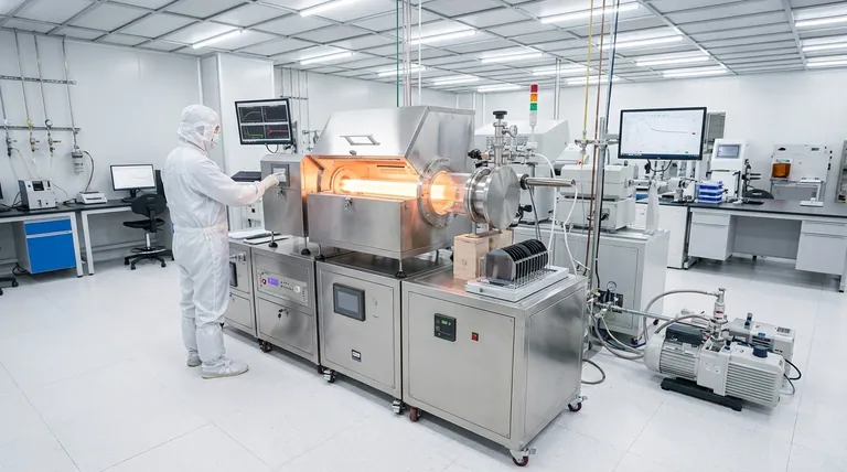
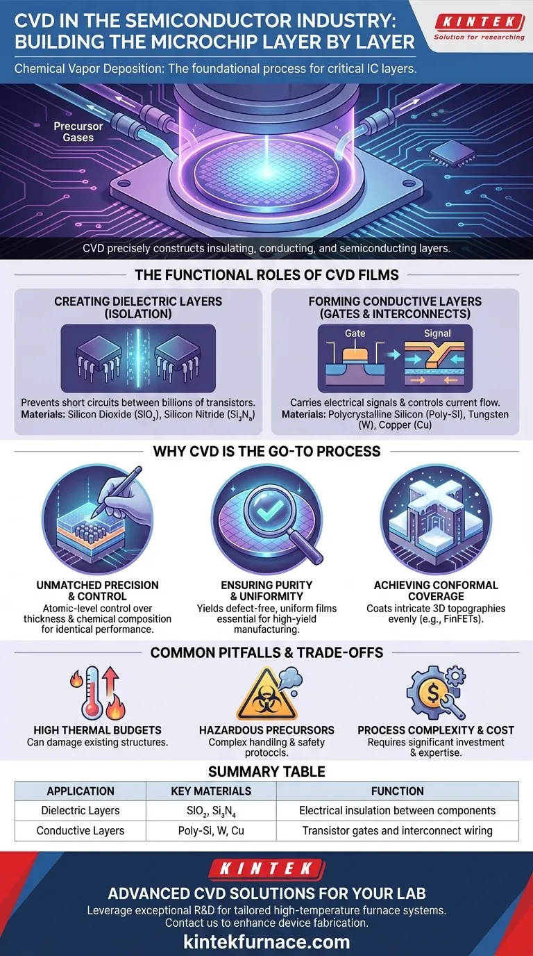
In the semiconductor industry, Chemical Vapor Deposition (CVD) is the foundational process used to build the critical layers of an integrated circuit. Its most common applications are the deposition of thin films like silicon dioxide (SiO₂) and silicon nitride (Si₃N₄) for electrical insulation, polycrystalline silicon (poly-Si) for transistor gates, and metals like tungsten for creating conductive pathways.
At its core, CVD isn't just about applying coatings; it's about precisely constructing the fundamental building blocks of a microchip. The process allows for the creation of the distinct insulating, conducting, and semiconducting layers that define modern electronic devices.
The Functional Roles of CVD Films in an Integrated Circuit
To understand CVD's importance, you must look at the specific function each deposited layer performs within a transistor, the basic switch that powers all digital logic.
Creating Dielectric Layers for Isolation
The most frequent use of CVD is to deposit dielectric (insulating) films. Billions of transistors are packed onto a single chip, and they must be electrically isolated from one another to prevent short circuits.
CVD is used to grow films of silicon dioxide (SiO₂) and silicon nitride (Si₃N₄). These materials act as the primary insulators between conductive components, ensuring that electrical signals travel only along their intended paths.
Forming Conductive Layers for Gates and Interconnects
CVD is also essential for creating the pathways that carry electrical signals and control the flow of current.
Polycrystalline silicon (poly-Si) is a key material deposited via CVD to form the gate of a transistor. The gate acts as the switch that turns the transistor on or off.
Additionally, CVD is used to deposit metals like tungsten (W) and copper (Cu). These metals fill tiny trenches and vias to form the intricate "wiring," or interconnects, that link millions or billions of transistors together into a functional circuit.
Why CVD is the Go-To Process
CVD is favored over other deposition methods in semiconductor manufacturing because it provides an unparalleled level of control, which is non-negotiable at the nanometer scales of modern chips.
Unmatched Precision and Control
CVD allows for atomic-level control over the thickness and chemical composition of the deposited film. This precision is critical for ensuring that every transistor on a chip performs identically.
Ensuring Purity and Uniformity
The process yields exceptionally uniform and defect-free films across the entire surface of a silicon wafer. A single microscopic defect can render an entire multi-million-dollar chip useless, making the purity and consistency of CVD essential for manufacturing yield and device reliability.
Achieving Conformal Coverage
As transistors have shrunk, they have evolved into complex three-dimensional structures (like FinFETs). CVD excels at creating conformal films, meaning the deposited material coats all surfaces of these intricate topographies evenly, much like how a layer of snow blankets an entire landscape.
Common Pitfalls and Trade-offs
While indispensable, CVD is not without its complexities. Understanding its limitations provides a more complete picture of the fabrication process.
High Thermal Budgets
Many CVD processes, particularly those for high-quality films like silicon nitride, require very high temperatures. This "thermal budget" can potentially damage or alter other structures already present on the wafer, forcing engineers to carefully sequence manufacturing steps.
Precursor Chemistry and Safety
CVD relies on volatile and often hazardous precursor gases. Managing the handling, delivery, and byproducts of these chemicals adds significant complexity and cost to the fabrication facility (fab). The choice of precursor directly impacts film quality, cost, and safety protocols.
Process Complexity and Cost
CVD reactors are highly sophisticated and expensive pieces of capital equipment. Developing and maintaining a stable, repeatable CVD process for a specific film requires significant investment in both equipment and engineering expertise.
Making the Right Choice for Your Goal
The specific CVD application is always tied directly to the functional requirement of the device being built.
- If your primary focus is electrical isolation: You will use CVD to deposit dielectric films like silicon dioxide or silicon nitride between conductive elements.
- If your primary focus is creating conductive pathways: You will use CVD to deposit polycrystalline silicon for transistor gates or metals like tungsten for interconnect wiring.
- If your primary focus is building the active device: You will use CVD to deposit the core semiconducting materials, like polysilicon, that form the heart of the transistor itself.
Ultimately, CVD is the technology that translates the architectural blueprint of a chip into a physical, functional reality, layer by atomic layer.
Summary Table:
| Application | Key Materials Deposited | Function in Semiconductor Devices |
|---|---|---|
| Dielectric Layers | Silicon Dioxide (SiO₂), Silicon Nitride (Si₃N₄) | Electrical insulation between components |
| Conductive Layers | Polycrystalline Silicon (poly-Si), Tungsten (W), Copper (Cu) | Transistor gates and interconnect wiring |
| General Benefits | Various thin films | Precision, uniformity, and conformal coverage for high-yield manufacturing |
Need advanced CVD solutions for your semiconductor lab? KINTEK leverages exceptional R&D and in-house manufacturing to provide high-temperature furnace solutions like CVD/PECVD Systems, Muffle, Tube, Rotary, Vacuum & Atmosphere Furnaces. Our strong deep customization capability ensures precise alignment with your unique experimental needs. Contact us today to enhance your device fabrication with reliable, tailored equipment!
Visual Guide
Related Products
- Custom Made Versatile CVD Tube Furnace Chemical Vapor Deposition CVD Equipment Machine
- Multi Heating Zones CVD Tube Furnace Machine for Chemical Vapor Deposition Equipment
- HFCVD Machine System Equipment for Drawing Die Nano Diamond Coating
- Split Chamber CVD Tube Furnace with Vacuum Station CVD Machine
- 915MHz MPCVD Diamond Machine Microwave Plasma Chemical Vapor Deposition System Reactor
People Also Ask
- Why are CVD tube furnace sintering systems indispensable for 2D material research and production? Unlock Atomic-Scale Precision
- How might AI and machine learning enhance CVD tube furnace processes? Boost Quality, Speed, and Safety
- Which industries and research fields benefit from CVD tube furnace sintering systems for 2D materials? Unlock Next-Gen Tech Innovations
- How does CVD tube furnace sintering enhance graphene growth? Achieve Superior Crystallinity and High Electron Mobility
- What temperature range do standard CVD tube furnaces operate at? Unlock Precision for Your Material Deposition


