High-temperature annealing is the critical "activation" step required to transform Indium-doped Copper Oxide from a raw, deposited layer into a functional semiconductor. Specifically, heating the film to 300°C in an industrial-grade furnace provides the thermal energy needed to repair the structural disorder caused during deposition, allowing Indium ions to integrate correctly into the crystal lattice.
The Core Insight Deposition leaves thin films in a stressed, disordered state that inhibits performance. Annealing is not merely a drying process; it is a structural reorganization that eliminates residual stress and locks dopant ions into their correct lattice positions, unlocking the material's electrical and optical potential.
The Structural Transformation
The primary purpose of annealing Indium-doped Copper Oxide is to move the material from a chaotic, as-deposited state to an ordered crystalline state.
Enhancing Crystalline Quality
When thin films are first deposited, the atoms often land in random, disordered arrangements. Annealing at 300°C provides the kinetic energy required for these atoms to migrate and rearrange themselves. This transition creates a robust crystal structure, which is the foundation for consistent electronic performance.
Eliminating Residual Stresses
The physical process of deposition forces atoms onto a substrate, generating significant internal tension. If left untreated, this residual stress can lead to mechanical failure, such as cracking or delamination. Thermal treatment relaxes the film, releasing these internal forces and mechanically stabilizing the layer.
Improving Grain Connectivity
For electrons to flow through a material, they must navigate the boundaries between individual crystal grains. Annealing improves the connectivity between these grains, reducing the barriers that usually impede electron flow. Better connectivity directly translates to more efficient electrical transport across the film.
Activating Electronic Properties
Beyond structural repair, the furnace treatment is essential for "activating" the chemical properties that make the film useful.
Effective Ion Placement
Doping Copper Oxide with Indium only works if the Indium atoms sit in specific spots within the Copper Oxide lattice. Without heat, Indium ions may remain stuck in interstitial spaces where they cannot contribute effectively. Annealing forces the effective placement of Indium ions into the lattice structure, integrating them as active dopants.
Optimizing Carrier Concentration
Once the Indium ions are correctly positioned, they can release charge carriers (electrons or holes) into the material. This process optimizes the carrier concentration, which is the primary metric for how well a semiconductor can conduct electricity. Without this step, the material would likely behave more like an insulator than a doped semiconductor.
Boosting Photoluminescence
The orderly lattice and improved grain structure also enhance how the material interacts with light. By reducing structural defects that typically trap and waste energy, the film achieves higher photoluminescence efficiency. This makes the material far more effective for optoelectronic applications.
Understanding the Trade-offs
While annealing is necessary, it is a process defined by a specific "thermal budget."
The Risk of Over-Processing
While the target for Indium-doped Copper Oxide is 300°C, varying from this temperature can have detrimental effects. Excessive heat or prolonged duration can induce unwanted phase changes or cause dopants to diffuse out of the film entirely. Conversely, insufficient heat will fail to fully crystallize the material, leaving it with high resistance and poor optical clarity.
Material Specificity
It is vital to note that "high temperature" is relative to the material. While Indium-doped Copper Oxide requires 300°C, other materials like Boron Tin Oxide or Molybdenum Disulfide may require temperatures ranging from 750°C to 900°C to achieve similar effects. Applying the wrong thermal profile to your specific oxide can degrade the film rather than enhance it.
Making the Right Choice for Your Goal
The annealing process must be tailored to the specific performance metric you are trying to maximize.
- If your primary focus is Electrical Conductivity: Prioritize the temperature accuracy (300°C) to ensure Indium ions are correctly seated in the lattice, maximizing carrier concentration.
- If your primary focus is Mechanical Stability: Focus on the duration of the anneal to ensure complete relaxation of residual stresses, preventing future delamination.
- If your primary focus is Optical Efficiency: Ensure the furnace atmosphere is controlled to maximize grain connectivity, which minimizes the scattering of charge carriers and light.
Successful annealing turns a fragile, resistive coating into a robust, high-performance component ready for device integration.
Summary Table:
| Optimization Goal | Key Mechanism | Furnace Requirement |
|---|---|---|
| Structural Integrity | Stress relaxation & grain growth | Precise temperature soak time |
| Electrical Conductivity | Indium ion lattice integration | Uniform 300°C heat distribution |
| Optical Performance | Defect reduction & photoluminescence | Controlled heating environment |
| Mechanical Stability | Elimination of residual stress | Gradual thermal ramp-down |
Maximize Your Material Performance with KINTEK
Achieving the precise 300°C thermal budget for Indium-doped Copper Oxide requires absolute temperature uniformity and control. Backed by expert R&D and manufacturing, KINTEK offers specialized Muffle, Tube, Rotary, Vacuum, and CVD systems designed to meet the rigorous demands of semiconductor research. Whether you need a standard solution or a system fully customizable for unique thin-film needs, our lab high-temp furnaces ensure your materials reach their full electrical and optical potential.
Ready to elevate your thin-film research? Contact KINTEK today for a customized furnace solution.
References
- Structural and Optical Modifications of Indium‐Doped Copper Oxide (CuO) Thin Films Synthesized by Chemical Bath Deposition for Enhanced Photoluminescence. DOI: 10.1002/nano.70050
This article is also based on technical information from Kintek Furnace Knowledge Base .
Related Products
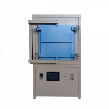
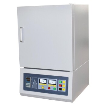
- High Temperature Muffle Oven Furnace for Laboratory Debinding and Pre Sintering
- Vacuum Heat Treat Sintering Furnace Molybdenum Wire Vacuum Sintering Furnace
- Vertical Laboratory Quartz Tube Furnace Tubular Furnace
- 1400℃ Controlled Inert Nitrogen Atmosphere Furnace
- Laboratory Muffle Oven Furnace with Bottom Lifting
People Also Ask
- What role does a high-temperature muffle furnace play in STFO synthesis? Achieve Pure Perovskite Results
- What role does a high-temperature muffle furnace play in TiO2 and PEN cross-linking? Unlock High-Performance Hybrids
- What is the function of a high-temperature muffle furnace in Belite research? Optimize Polymorphic Phase Transitions
- What is the primary function of a high-temperature muffle furnace for cerium dioxide precursors? Expert Calcination Tips
- How does precise temperature control affect MoS2/rGO hybrids? Mastering Nanowall Morphology