Encapsulation acts as a critical survival mechanism for the material. During the rigorous high-temperature annealing process, layers like hexagonal Boron Nitride (hBN) or graphene serve as an atomic-level shield, physically isolating the monolayer Transition Metal Dichalcogenide (TMD) to prevent it from chemically reacting with the surrounding environment.
High-temperature annealing is necessary to repair lattice defects, but the heat renders exposed TMDs vulnerable to degradation. Encapsulation resolves this conflict by providing a protective, ultra-flat barrier that allows for effective lattice repair while suppressing substrate interference.
The Necessity of Environmental Isolation
Preventing Chemical Degradation
High-temperature annealing is required to fix structural defects in TMDs, but elevated temperatures significantly increase the material's reactivity.
Without protection, the monolayer TMD is exposed to the atmosphere, leading to oxidation and material degradation that destroys its electronic properties.
Creating an Atomic-Level Barrier
Encapsulation layers like hBN and graphene act as physical barriers at the atomic scale.
This isolation ensures that the TMD remains chemically pristine, allowing the thermal energy to focus on lattice repair rather than fueling destructive chemical reactions.
The Role of Interface Quality
Providing an Ultra-Flat Surface
Standard substrates often possess microscopic roughness that strains the atomically thin TMD.
hBN provides an ultra-flat interface that supports the TMD without introducing mechanical stress, ensuring the material remains structurally uniform during the heating process.
Suppressing Substrate Scattering
Beyond physical smoothness, the interface between the TMD and the substrate is a common source of electronic interference.
Encapsulation creates an environment free of charge impurities. This suppression of scattering from the underlying substrate is essential for preserving the intrinsic properties of the semiconductor.
Maximizing Electronic and Optical Performance
Facilitating Lattice Repair and De-doping
The protective environment created by encapsulation allows the annealing process to effectively heal defects in the crystal lattice.
Simultaneously, it maximizes de-doping effects, removing unwanted charge carriers that often compromise the material's performance.
Enhancing Photoluminescence
The combination of a repaired lattice and a clean, scattering-free interface leads to tangible performance gains.
Specifically, these factors combine to significantly enhance the photoluminescence quantum yield (PL QY), making the material far more efficient at emitting light.
Understanding the Trade-offs
Process Complexity vs. Performance
While encapsulation is required for protection during high-heat treatments, it introduces additional steps to the fabrication process.
You must create a "sandwich" structure (heterostructure) with precision, which is more complex than simply depositing a TMD on a silicon wafer.
The Cost of "Naked" Annealing
The alternative—annealing without encapsulation—severely limits the temperatures you can use.
Without the cap, you cannot reach the thermal thresholds necessary for deep lattice repair without destroying the material, resulting in lower-quality samples with higher defect densities.
Making the Right Choice for Your Project
Encapsulation is not merely a protective step; it is an enhancement technique that defines the final quality of your material.
- If your primary focus is optical efficiency: You must use hBN encapsulation to suppress scattering and maximize photoluminescence quantum yield.
- If your primary focus is defect reduction: You require encapsulation to safely reach the high temperatures needed for effective lattice repair and de-doping without degrading the sample.
Ultimately, encapsulation transforms annealing from a destructive risk into a highly effective purification process.
Summary Table:
| Feature | Effect of Encapsulation | Impact on TMD Material |
|---|---|---|
| Atmospheric Shielding | Blocks oxygen and contaminants | Prevents chemical degradation/oxidation |
| Interface Quality | Provides an ultra-flat hBN surface | Eliminates mechanical stress & roughness |
| Charge Environment | Suppresses substrate scattering | Removes charge impurities & de-dopes material |
| Thermal Stability | Allows higher annealing temperatures | Enables deep lattice repair without sample loss |
| Optical Performance | Maximizes PL Quantum Yield | Significantly enhances light emission efficiency |
Elevate Your 2D Material Research with KINTEK
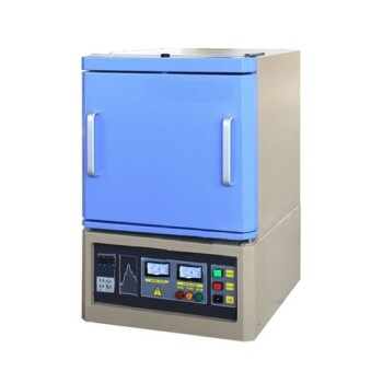
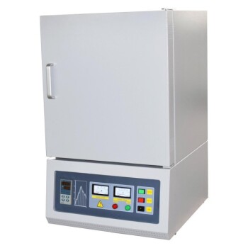
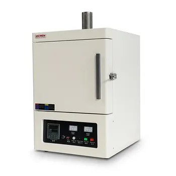
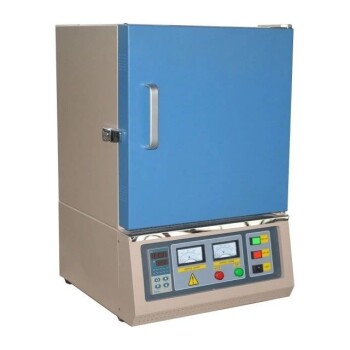
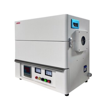
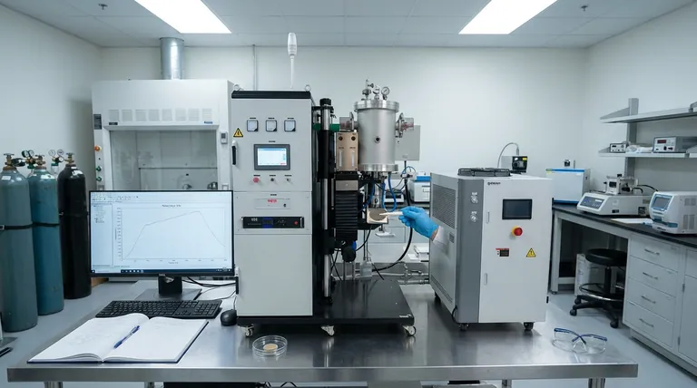
Precise high-temperature annealing requires more than just protection—it demands the right thermal environment. KINTEK provides industry-leading Muffle, Tube, Vacuum, and CVD systems designed to meet the rigorous standards of semiconductor and 2D material research.
Backed by expert R&D and manufacturing, our customizable laboratory furnaces ensure the temperature uniformity and atmosphere control necessary to maximize the benefits of hBN and graphene encapsulation.
Ready to achieve superior lattice repair and optical performance? Contact our experts today to find the perfect thermal solution for your lab.
References
- Huije Ryu, Gwan‐Hyoung Lee. Optical grade transformation of monolayer transition metal dichalcogenides <i>via</i> encapsulation annealing. DOI: 10.1039/d3nr06641j
This article is also based on technical information from Kintek Furnace Knowledge Base .
Related Products
- 2200 ℃ Tungsten Vacuum Heat Treat and Sintering Furnace
- High Temperature Muffle Oven Furnace for Laboratory Debinding and Pre Sintering
- 1700℃ Controlled Inert Nitrogen Atmosphere Furnace
- 1800℃ High Temperature Muffle Oven Furnace for Laboratory
- 1400℃ High Temperature Laboratory Tube Furnace with Alumina Tube
People Also Ask
- What role does a high-temperature vacuum sintering furnace play in the densification of WC-10(Ni, Ni/Co) alloys?
- How does a tungsten-heated vacuum sintering furnace prepare (TbxY1-x)2O3 ceramics? Achieve 99%+ Density & Purity
- What core role does a high-temperature vacuum sintering furnace play in Sm:YAG ceramics? Mastering Optical Clarity
- What are the benefits of using vacuum heat treating furnaces for metal alloys? Achieve Superior Metal Properties and Performance
- What is the significance of a high-temperature vacuum sintering furnace? Achieving Ho:Y2O3 Optical Transparency