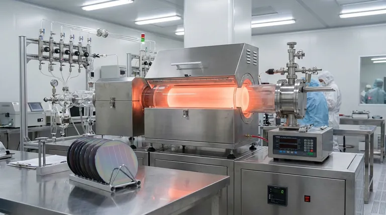
Atomic Layer Deposition (ALD) equipment is essential for creating the ultra-thin, dense aluminum oxide (Al2O3) layers required for high-efficiency silicon solar cells. By depositing these precise films, the equipment provides negative charge field passivation, which is the primary mechanism for reducing energy loss at the rear of the cell.
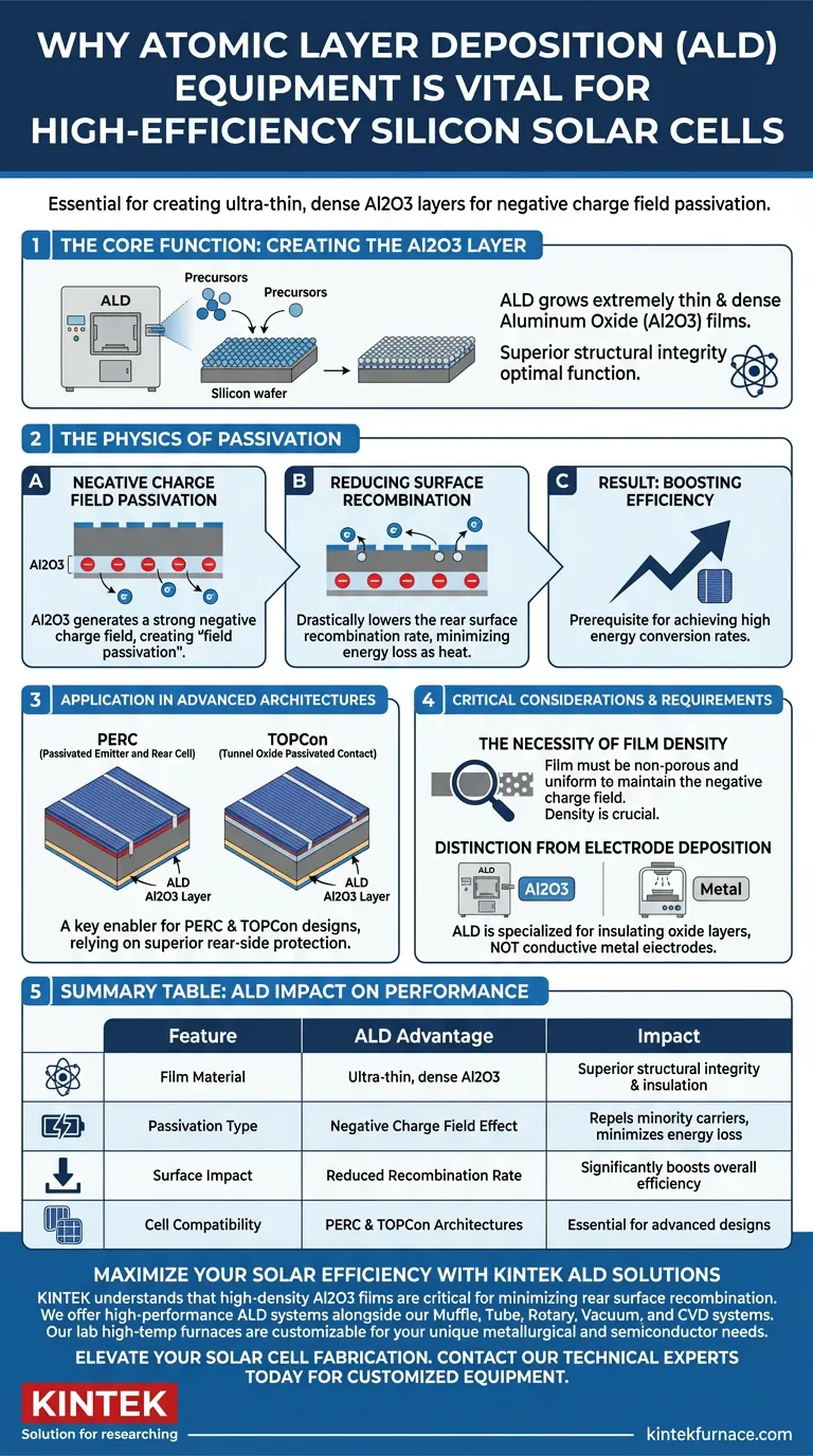
The core value of ALD lies in its ability to grow high-quality Al2O3 films that introduce a negative charge field. This field shields the rear surface, significantly lowering the recombination rate and boosting the efficiency of advanced architectures like PERC and TOPCon.
The Physics of Passivation
Creating the Al2O3 Layer
The primary function of ALD equipment in this context is to grow aluminum oxide (Al2O3) films.
Unlike other deposition methods, ALD is capable of producing films that are extremely thin and dense. This structural integrity is vital for the layer to function correctly within the solar cell stack.
Negative Charge Field Passivation
The specific advantage of using Al2O3 on upgraded metallurgical grade silicon is the generation of a negative charge field.
This field effect provides what is known as "field passivation." It effectively repels minority carriers from the rear interface, preventing them from recombining and being lost as heat.
Reducing Surface Recombination
By repelling carriers via this negative field, the ALD-grown layer drastically reduces the rear surface recombination rate.
Minimizing this recombination is a prerequisite for achieving high energy conversion rates in modern silicon cells.
Application in Advanced Architectures
Enabling PERC and TOPCon
The capabilities of ALD are not just theoretical; they are a manufacturing requirement for specific high-efficiency designs.
Specifically, this technology is a key enabler for PERC (Passivated Emitter and Rear Cell) and TOPCon (Tunnel Oxide Passivated Contact) structures. These advanced designs rely on the superior rear-side protection that only high-quality ALD films can provide.
Critical Considerations and Requirements
The Necessity of Film Density
While ALD is powerful, its effectiveness relies entirely on the quality of the film it produces.
The Al2O3 layer must be sufficiently dense to maintain the negative charge field. If the equipment fails to produce a non-porous, uniform layer, the passivation effect will be compromised, and the efficiency gains will be lost.
Distinction from Electrode Deposition
It is important to distinguish the role of ALD from other deposition processes in solar cell fabrication.
While ALD handles the passivation layer, other systems (such as vacuum evaporation) are typically required to deposit metal electrodes (like gold) for ohmic contacts. ALD is specialized strictly for the insulating and passivating oxide layers, not the conductive metal contacts.
Making the Right Choice for Your Goal
To maximize the performance of upgraded metallurgical grade silicon cells, consider the following:
- If your primary focus is reducing energy loss: Prioritize ALD processes that guarantee high-density Al2O3 films to maximize negative charge field passivation.
- If your primary focus is architectural upgrades (PERC/TOPCon): Ensure your ALD equipment is calibrated to produce the extremely thin layers required to fit within these complex cell structures without impeding optical performance.
Ultimately, the precision of your ALD process in growing dense Al2O3 layers is the defining factor in minimizing rear recombination and achieving high-efficiency targets.
Summary Table:
| Feature | ALD Process Advantage | Impact on Solar Cell Performance |
|---|---|---|
| Film Material | Ultra-thin, dense Aluminum Oxide (Al2O3) | Provides superior structural integrity and insulation |
| Passivation Type | Negative Charge Field Effect | Repels minority carriers to minimize energy loss |
| Surface Impact | Reduced Recombination Rate | Significantly boosts overall energy conversion efficiency |
| Cell Compatibility | PERC and TOPCon Architectures | Essential for manufacturing advanced high-efficiency designs |
Maximize Your Solar Efficiency with KINTEK ALD Solutions
Precision at the atomic level is the difference between standard performance and industry-leading efficiency. At KINTEK, we understand that high-density Al2O3 films are critical for minimizing rear surface recombination in PERC and TOPCon architectures.
Backed by expert R&D and manufacturing, KINTEK offers high-performance ALD systems alongside our Muffle, Tube, Rotary, Vacuum, and CVD systems. Our lab high-temp furnaces are fully customizable to meet your unique metallurgical and semiconductor needs, ensuring your upgraded silicon cells achieve their maximum potential.
Ready to elevate your solar cell fabrication? Contact our technical experts today to discuss your customized equipment requirements!
Visual Guide
References
- Production of upgraded metallurgical-grade silicon for a low-cost, high-efficiency, and reliable PV technology. DOI: 10.3389/fphot.2024.1331030
This article is also based on technical information from Kintek Furnace Knowledge Base .
Related Products
- High Temperature Muffle Oven Furnace for Laboratory Debinding and Pre Sintering
- 1400℃ High Temperature Laboratory Tube Furnace with Alumina Tube
- 1700℃ High Temperature Laboratory Tube Furnace with Alumina Tube
- Multi Zone Laboratory Quartz Tube Furnace Tubular Furnace
- Vertical Laboratory Quartz Tube Furnace Tubular Furnace
People Also Ask
- Why is controlled heat treatment in a muffle furnace necessary for calcined clay? Achieve Optimal Pozzolanic Activity
- What is the function of a laboratory high-temperature muffle furnace in niobate phosphor synthesis?
- What role does a high-temperature muffle furnace play in TiO2 and PEN cross-linking? Unlock High-Performance Hybrids
- How does a high-temperature muffle furnace convert shell powder to CaO? Achieve High-Purity Calcium Oxide via Calcination
- What is the primary function of a high-temperature muffle furnace for cerium dioxide precursors? Expert Calcination Tips


