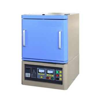
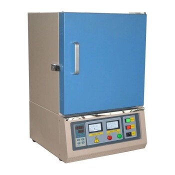
A laboratory high-temperature annealing furnace is essential to transform a raw, solution-processed coating into a functional semiconductor. This equipment provides the precise thermal environment necessary to drive crystallization and evaporate residual solvents, ensuring the film achieves the structural integrity required for high performance.
The annealing process is the critical bridge between a raw chemical precursor and a working device; it dictates grain size, reduces defects, and defines the final photoelectric conversion efficiency.
Orchestrating the Phase Transition
From Amorphous to Crystalline
Initially, a spin-coated perovskite film often exists in a disordered or amorphous state. The annealing furnace provides the thermal energy required to trigger atomic diffusion and rearrangement.
This energy input drives the material to reorganize itself into a stable polycrystalline structure. Without this step, the material lacks the ordered lattice required for effective electron transport.
Optimizing Grain Growth
The specific temperature and duration of the anneal control how crystals nucleate and grow. Precise regulation allows you to optimize the grain size of the material.
Larger grains generally result in fewer grain boundaries, which are common traps for electrical charge. By maximizing grain size, you improve the film’s overall crystallinity and electronic connectivity.
Ensuring Film Purity and Integrity
Eliminating Residual Solvents
Wet chemical deposition leaves behind organic solvents and precursors within the film lattice. High-temperature treatment promotes the complete evaporation of these residual solvents.
Removing these impurities is vital for converting the initial sol-gel structure into a solid state. This prevents the formation of voids and ensures the film remains chemically pure.
Enhancing Surface Coverage
A successful anneal improves the physical coverage of the film across the substrate. As the material crystallizes and solvents leave, the film densifies.
This results in a continuous, uniform layer that prevents electrical shorts between device layers.
Reducing Internal Defects
Crystallization is not just about structure; it is about healing. The thermal energy helps resolve lattice distortions and reduces internal defects.
Lowering the defect density is the primary driver for enhancing the photoelectric conversion efficiency, allowing the device to convert light into electricity more effectively.
Understanding the Trade-offs
The Balance of Temperature
While heat is necessary for formation, excessive temperatures can be destructive. Over-annealing may lead to the decomposition of the perovskite crystal structure or the evaporation of volatile components.
Atmosphere Control
High temperatures increase chemical reactivity. As noted in semiconductor processing, oxidizing environments can degrade thin film properties.
Using a furnace with a controlled atmosphere (such as inert Argon gas) is often necessary to prevent oxidation while driving the crystallization process.
Making the Right Choice for Your Goal
To maximize the potential of your perovskite thin films, tailor your annealing profile to your specific objectives:
- If your primary focus is Device Efficiency: Prioritize optimizing the temperature profile to maximize grain size and crystallinity, as this minimizes charge recombination.
- If your primary focus is Film Stability: Ensure the duration is sufficient to fully remove residual solvents, which can otherwise act as degradation pathways over time.
By controlling the thermal history of your film, you determine the ultimate limit of its performance.
Summary Table:
| Feature | Impact on Perovskite Thin Film |
|---|---|
| Crystallization Control | Drives atomic diffusion to transform amorphous precursors into ordered lattices. |
| Grain Size Optimization | Maximizes grain growth to reduce charge-trapping boundaries. |
| Solvent Removal | Evaporates residual organic solvents to prevent voids and chemical impurities. |
| Defect Reduction | Heals lattice distortions to boost photoelectric conversion efficiency. |
| Atmosphere Regulation | Prevents oxidation and material degradation during high-heat cycles. |
Elevate Your Perovskite Research with KINTEK
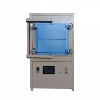
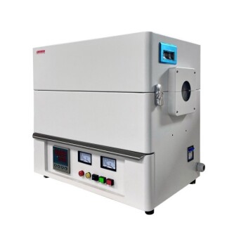
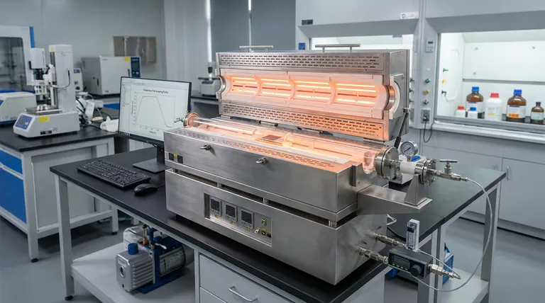
Precise thermal control is the difference between a raw precursor and a high-performance semiconductor. KINTEK provides world-class laboratory high-temperature furnaces—including Muffle, Tube, Rotary, Vacuum, and CVD systems—specifically designed to meet the rigorous demands of thin-film annealing.
Backed by expert R&D and precision manufacturing, our systems are fully customizable to your unique research needs, ensuring uniform grain growth and optimal film integrity. Don’t let thermal inconsistencies limit your device efficiency.
Contact KINTEK today to find your perfect custom furnace solution.
References
- Maoding Cheng, Qinglong Jiang. Progress and Application of Halide Perovskite Materials for Solar Cells and Light Emitting Devices. DOI: 10.3390/nano14050391
This article is also based on technical information from Kintek Furnace Knowledge Base .
Related Products
- 1400℃ High Temperature Laboratory Tube Furnace with Alumina Tube
- 1700℃ High Temperature Laboratory Tube Furnace with Alumina Tube
- 1800℃ High Temperature Muffle Oven Furnace for Laboratory
- 1700℃ High Temperature Muffle Oven Furnace for Laboratory
- 1200℃ Muffle Oven Furnace for Laboratory
People Also Ask
- What role do high-performance box or tube furnaces play in LATP sintering? Master Densification & Ionic Conductivity
- How does a laboratory high-temperature tube furnace contribute to the conversion of electrospun fibers? Expert Insights
- How do high-temperature laboratory tube furnaces ensure environmental stability? Precision Thermal Reduction Tips
- What is the function of a furnace in CuAlMn alloy treatment? Achieve Perfect Microstructural Homogenization
- In what scenarios are laboratory high-temperature tube furnaces or muffle furnaces utilized? Study MgTiO3-CaTiO3 Ceramics