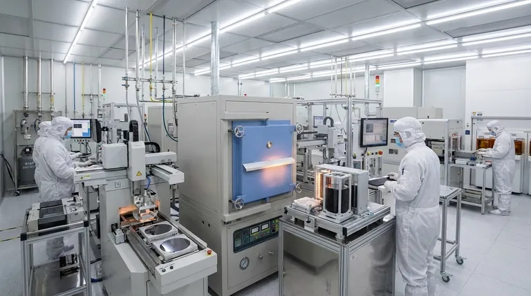
In the electronics sector, atmosphere furnaces are the cornerstone of semiconductor fabrication. They create the hyper-controlled, oxygen-free environments necessary to manufacture the microchips at the heart of nearly every modern device. Key processes like doping, diffusion, and annealing all rely on these furnaces to precisely alter the electrical properties of silicon wafers without introducing catastrophic contamination.
The fundamental challenge in electronics manufacturing is not just building small components, but manipulating the atomic properties of materials with absolute purity. Atmosphere furnaces are the critical technology that makes this possible, serving as pristine environments where the fundamental building blocks of integrated circuits are forged.
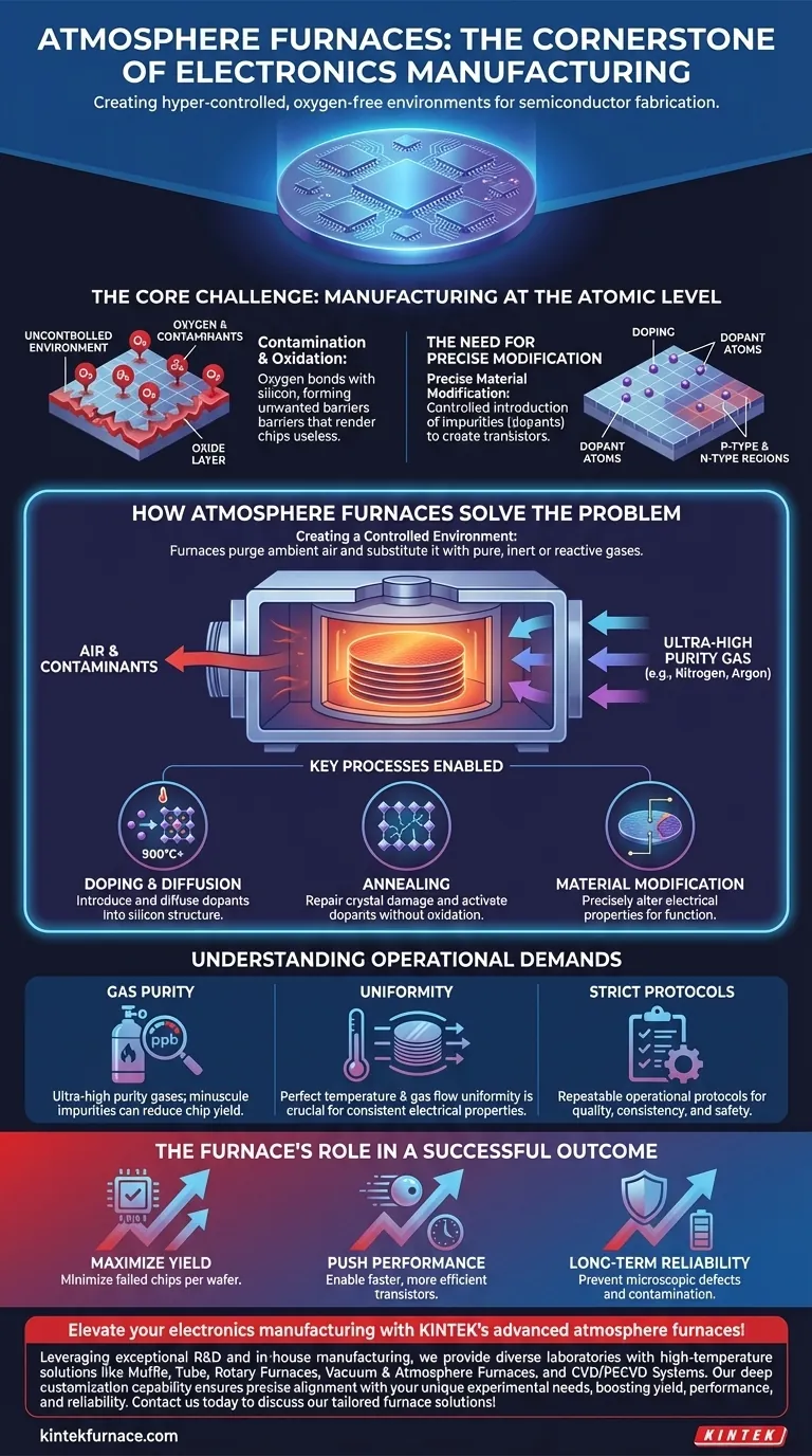
The Core Challenge: Manufacturing at the Atomic Level
Modern electronics operate on a scale where a single misplaced atom can cause a device to fail. The entire semiconductor manufacturing process is a battle against environmental contamination and physical imperfection.
The Problem of Contamination
An integrated circuit is built layer by layer on a silicon wafer. During high-temperature processing, reactive gases in the air—especially oxygen—will readily bond with the silicon, forming an unwanted layer of silicon dioxide.
This unintended oxidation can block the introduction of necessary elements or create insulating barriers where conductive paths should be, rendering the chip useless.
The Need for Precise Material Modification
A pure silicon wafer is not a useful semiconductor on its own. Its ability to conduct electricity must be precisely modified in specific areas.
This process, known as doping, involves introducing a tiny, controlled number of impurity atoms (dopants) into the silicon crystal lattice. This is what creates the "p-type" and "n-type" regions that form transistors, the basic on/off switches of digital logic.
How Atmosphere Furnaces Solve the Problem
An atmosphere furnace is fundamentally a chamber where temperature and the gaseous environment are controlled with extreme precision. Its primary job is to eliminate the unpredictable ambient air and substitute it with a specific, pure gas mixture.
Creating a Controlled Environment
The furnace is first purged of air and then filled with either an inert gas, like nitrogen or argon, which will not react with the silicon, or a specific reactive gas that is part of the intended chemical process.
This controlled atmosphere ensures that the only chemical reactions occurring are the ones designed by the engineers.
Key Processes Enabled by This Control
Doping and Diffusion: To introduce dopants, wafers are placed in the furnace along with the dopant source. At high temperatures (often over 900°C), the dopant atoms gain enough energy to move, or diffuse, into the silicon crystal structure. The controlled atmosphere ensures only the desired dopants are introduced.
Annealing: After processes like ion implantation (another doping method) damage the silicon's crystal structure, the wafer must be heated in a process called annealing. This allows the crystal lattice to repair itself and properly "activate" the dopants. Performing this in an atmosphere furnace prevents the wafer from oxidizing during this critical healing phase.
Understanding the Operational Demands
The effectiveness of an atmosphere furnace in electronics is not guaranteed. It depends on meeting extraordinarily high standards of operational control, where there is virtually no margin for error.
The Unforgiving Nature of Gas Purity
The gases used, such as nitrogen and argon, must be of ultra-high purity, often measured in parts per billion. Even minuscule impurities in the gas supply can be a source of contamination that reduces the yield of functional chips from each wafer.
The Tyranny of Uniformity
The temperature and gas flow must be perfectly uniform across every wafer in the furnace, and from one batch to the next. Any temperature variation can cause dopants to diffuse at different rates, leading to inconsistent electrical properties across the chip and a failed device.
Strict Protocols are Non-Negotiable
Maintaining the furnace—from cleaning the chamber to calibrating sensors and managing gas lines—is critical. Strict, repeatable operational protocols are essential for ensuring process quality, consistency, and the safety of handling high temperatures and specialty gases.
The Furnace's Role in a Successful Outcome
The function of the atmosphere furnace is directly tied to the three primary goals of semiconductor manufacturing: yield, performance, and reliability.
- If your primary focus is maximizing production yield: The furnace's most important job is providing absolute atmosphere purity and perfect temperature uniformity to minimize the number of failed chips per wafer.
- If your primary focus is pushing device performance: The furnace must enable precise, repeatable doping and annealing cycles that create the exact electrical properties required for faster, more efficient transistors.
- If your primary focus is long-term device reliability: The furnace serves to prevent the microscopic defects and contamination that, while not causing immediate failure, can lead to device breakdown over its operational lifespan.
Ultimately, the atmosphere furnace is not merely a piece of heating equipment; it is the foundational environment that enables the atomic-level engineering of modern electronics.
Summary Table:
| Aspect | Role in Electronics Sector |
|---|---|
| Core Function | Creates controlled, oxygen-free environments for semiconductor processes |
| Key Processes | Doping, diffusion, annealing to modify silicon wafer properties |
| Benefits | Prevents contamination, ensures uniform temperature, enhances chip performance and yield |
| Operational Demands | Requires ultra-high gas purity, strict protocols, and precise temperature control |
Elevate your electronics manufacturing with KINTEK's advanced atmosphere furnaces! Leveraging exceptional R&D and in-house manufacturing, we provide diverse laboratories with high-temperature solutions like Muffle, Tube, Rotary Furnaces, Vacuum & Atmosphere Furnaces, and CVD/PECVD Systems. Our deep customization capability ensures precise alignment with your unique experimental needs, boosting yield, performance, and reliability. Contact us today to discuss how our tailored furnace solutions can transform your semiconductor processes!
Visual Guide
Related Products
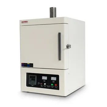
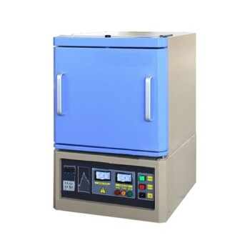
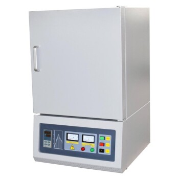
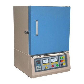
- Controlled Inert Nitrogen Hydrogen Atmosphere Furnace
- 1700℃ Controlled Inert Nitrogen Atmosphere Furnace
- 1200℃ Controlled Inert Nitrogen Atmosphere Furnace
- Mesh Belt Controlled Atmosphere Furnace Inert Nitrogen Atmosphere Furnace
- 9MPa Air Pressure Vacuum Heat Treat and Sintering Furnace
People Also Ask
- Why is controlled atmosphere capability important in an atmosphere furnace? Unlock Precise Material Processing
- What are the two major categories of controlled atmosphere furnaces? Choose Batch or Continuous for Your Needs
- What are the characteristics and uses of hydrogen atmosphere in furnaces? Achieve Superior Surface Purity and Bonding
- How does a controlled atmosphere furnace contribute to energy efficiency? Lower Costs with Advanced Thermal Management
- What Roles Do a Controlled Atmosphere Furnace and Oil Quenching Tank Play in AISI 5140 Steel Heat Treatment?