In short, a vast array of materials can be produced using Chemical Vapor Deposition (CVD). The process is not limited to one type of substance but is a versatile technique for creating high-performance solid films. Key materials include silicon-based compounds like silicon dioxide and nitride, various forms of carbon such as diamond and graphene, metallic coatings like tungsten and titanium nitride, and specialized high-κ dielectrics.
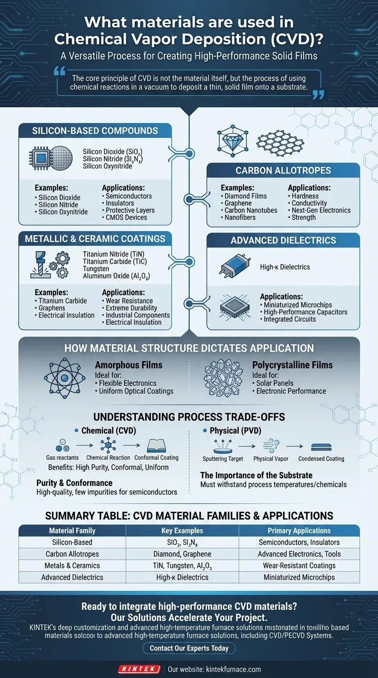
The core principle of CVD is not the material itself, but the process of using chemical reactions in a vacuum to deposit a thin, solid film onto a substrate. The specific material chosen is entirely dictated by the functional requirements of the final product, from a semiconductor chip to a wear-resistant cutting tool.
The Core Families of CVD Materials
CVD's versatility comes from its ability to handle distinct families of materials, each serving different industrial needs. The material deposited is formed from gaseous precursor molecules reacting on the surface of the item being coated.
Silicon-Based Compounds
This is the bedrock of the modern electronics industry. Materials like silicon dioxide (SiO₂), silicon nitride (Si₃N₄), and silicon oxynitride are deposited as thin films to act as insulators, protective layers, and dielectrics in the manufacturing of semiconductors and CMOS devices.
Carbon Allotropes
CVD is critical for producing advanced carbon structures with exceptional properties. This includes depositing diamond films for hardness, carbon nanotubes and nanofibers for strength and conductivity, and graphene for next-generation electronics.
Metallic and Ceramic Coatings
For applications requiring extreme durability, CVD is used to apply hard coatings. Common materials include titanium nitride (TiN), titanium carbide (TiC), and titanium carbonitride (TiCN), which provide excellent wear resistance for cutting tools and industrial components.
Tungsten and aluminum oxide (Al₂O₃) are also frequently deposited. Al₂O₃, in particular, is used as both a wear-resistant coating and an electrical insulator.
Advanced Dielectrics
In the quest for smaller and more powerful microchips, high-κ dielectrics are essential. CVD is a primary method for depositing these materials, which allow capacitors in integrated circuits to be miniaturized without losing capacitance.
How Material Structure Dictates Application
The same chemical material can be deposited with different internal structures, which fundamentally changes its properties and how it can be used.
Amorphous Films
CVD can produce amorphous materials, which lack a long-range crystalline structure. This disordered arrangement is often ideal for flexible electronics or optical coatings where uniformity is more important than crystal lattice perfection.
Polycrystalline Films
Conversely, the process can create polycrystalline films, which are composed of many small crystal grains. This structure is vital for applications like solar panels and many electronic devices where the specific crystalline properties are necessary for performance.
Understanding the Process Trade-offs
While powerful, CVD is a specific tool with its own context. Understanding its place among other deposition techniques is key to appreciating its value.
Chemical vs. Physical Deposition
CVD relies on a chemical reaction of precursor gases on a substrate surface. This is fundamentally different from Physical Vapor Deposition (PVD), which uses physical means like sputtering (e.g., with argon gas) to create a vapor that then condenses on the substrate. The chemical nature of CVD allows it to create highly pure and conformal coatings that perfectly cover complex shapes.
Purity and Conformance
A primary advantage of CVD is the ability to produce high-quality, high-purity films. Because the process is driven by chemical reactions from carefully controlled precursor gases, the resulting material has very few impurities. This is why it is indispensable in the semiconductor industry, where even trace contaminants can ruin a device.
The Importance of the Substrate
The final deposited material is only one part of the system. The choice of material and process parameters is heavily dependent on the substrate—the object being coated. The substrate must be able to withstand the temperatures and chemical environment of the CVD process without degrading.
Making the Right Choice for Your Application
To leverage CVD effectively, align the material choice with your primary technical goal.
- If your primary focus is semiconductor manufacturing: You will primarily work with silicon-based compounds (dioxide, nitride) and advanced high-κ dielectrics to build integrated circuits.
- If your primary focus is creating durable, wear-resistant coatings: Your materials of choice will be ceramics like titanium nitride (TiN), titanium carbide (TiC), and aluminum oxide (Al₂O₃) for tools and components.
- If your primary focus is advanced materials research: You should explore carbon allotropes like graphene, nanotubes, and diamond films for their unique electronic and structural properties.
Ultimately, CVD's power lies in its ability to transform gaseous chemicals into high-performance solid materials tailored for a specific function.
Summary Table:
| Material Family | Key Examples | Primary Applications |
|---|---|---|
| Silicon-Based | Silicon Dioxide (SiO₂), Silicon Nitride (Si₃N₄) | Semiconductors, Insulators, Protective Layers |
| Carbon Allotropes | Diamond, Graphene, Carbon Nanotubes | Advanced Electronics, Cutting Tools, Composites |
| Metals & Ceramics | Titanium Nitride (TiN), Tungsten, Aluminum Oxide (Al₂O₃) | Wear-Resistant Coatings, Industrial Tools |
| Advanced Dielectrics | High-κ Dielectrics | Miniaturized Microchips, High-Performance Capacitors |
Ready to integrate high-performance CVD materials into your research or production?
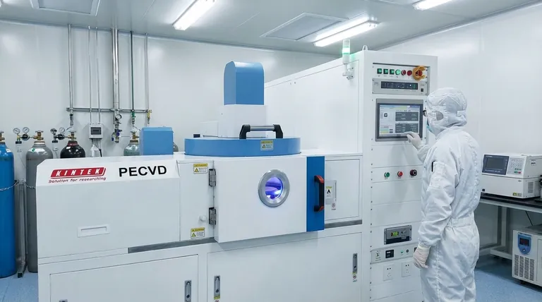
At KINTEK, we understand that your success depends on precise, reliable thin-film deposition. Our expertise in advanced high-temperature furnace solutions, including our specialized CVD/PECVD Systems, is matched by our strong deep customization capability. We work with you to tailor the equipment and process parameters to precisely meet your unique material requirements, whether you are developing next-generation semiconductors, ultra-hard coatings, or exploring novel materials like graphene.
Let's discuss how our solutions can accelerate your project. Contact our experts today for a personalized consultation.
Visual Guide
Related Products
- HFCVD Machine System Equipment for Drawing Die Nano Diamond Coating
- Custom Made Versatile CVD Tube Furnace Chemical Vapor Deposition CVD Equipment Machine
- 915MHz MPCVD Diamond Machine Microwave Plasma Chemical Vapor Deposition System Reactor
- Multi Heating Zones CVD Tube Furnace Machine for Chemical Vapor Deposition Equipment
- MPCVD Machine System Reactor Bell-jar Resonator for Lab and Diamond Growth
People Also Ask
- What is chemical vapor deposition (CVD) and its primary industrial application? Unlock Precision Thin Films for Electronics
- What role does Chemical Vapor Deposition (CVD) equipment play in the surface coating of carbon fibers for composites?
- What is the function of high-purity Argon (Ar) gas during CVD? Optimize Your Thin Film Uniformity and Purity
- How can customers maximize the quality of CVD coatings? Master Pre-Coating Prep for Superior Results
- What are the equipment for chemical vapor deposition? A Guide to the 5 Essential Components