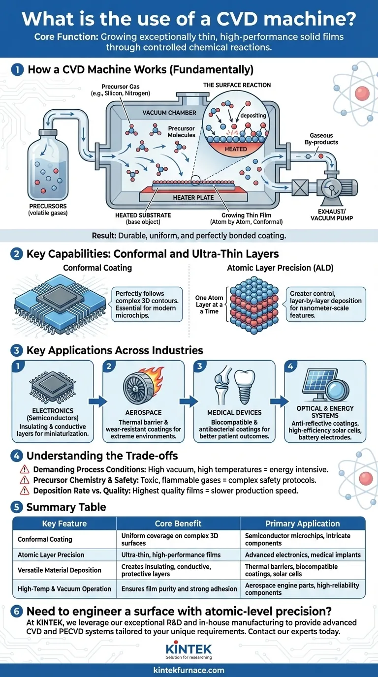
At its core, a Chemical Vapor Deposition (CVD) machine is used to grow exceptionally thin, high-performance films of solid material onto a surface. It accomplishes this not by painting or dipping, but by using controlled chemical reactions from gases to build a new layer, often just a few atoms thick. This process is fundamental to manufacturing the most advanced components in semiconductors, aerospace, and medicine.
The central purpose of CVD is to fundamentally alter the surface of an object, giving it new properties—like electrical insulation, heat resistance, or biocompatibility—that the underlying material does not possess. It enables the creation of materials with atomic-level precision, which is a requirement for most modern technology.
How a CVD Machine Fundamentally Works
To understand the use of a CVD machine, you must first understand its basic principle. It is a highly controlled process that takes place inside a vacuum chamber.
The Controlled Environment
The entire process occurs under vacuum, well below normal atmospheric pressure. A base object, known as the substrate, is placed inside the chamber and typically heated.
One or more volatile gases, called precursors, are then introduced into the chamber. These precursors contain the specific atoms needed for the final film (e.g., silicon, nitrogen, carbon).
The Surface Reaction
When the precursor gases come into contact with the heated substrate, they trigger a chemical reaction or decompose. This reaction causes the desired atoms to "deposit" or bond onto the substrate's surface, forming a solid film.
Building the Film, Atom by Atom
This deposition happens molecule-by-molecule, creating an extremely thin and uniform layer. Any unwanted by-products from the chemical reaction remain in a gaseous state and are pumped out of the chamber. The result is a durable, dry coating that is perfectly bonded to the substrate.
The Core Capability: Creating Conformal and Ultra-Thin Layers
The true power of CVD lies not just in creating thin films, but in the quality and precision of those films. This is what separates it from more traditional coating methods.
What “Conformal” Really Means
CVD creates conformal films, meaning the coating perfectly follows the contours of the substrate surface, no matter how complex or microscopic its features are. Think of it as a layer of paint that can cover every single nook and cranny of a three-dimensional microchip with perfect uniformity.
Pushing the Limits with Atomic Precision
A specialized form of this process, Atomic Layer Deposition (ALD), allows for even greater control, depositing a film literally one single layer of atoms at a time. This level of precision is essential for manufacturing modern semiconductor devices, where features are measured in nanometers.
Why This Is Impossible with Traditional Methods
Techniques like dipping, spraying, or electroplating cannot achieve this. They are unable to uniformly coat the complex, microscopic topographies found in integrated circuits or the intricate internal passages of advanced components.
Key Applications Across Industries
The ability to engineer surfaces at the atomic level makes CVD a critical technology in nearly every advanced industry.
Powering Modern Electronics
CVD is indispensable in semiconductor fabrication. It is used to deposit the ultra-thin insulating (silicon nitride) and conductive layers that make up integrated circuits, enabling the continuous miniaturization of computer chips.
Protecting High-Performance Components
In the aerospace industry, CVD applies thermal barrier coatings to turbine blades and other engine parts. These coatings protect the underlying metal from extreme temperatures, dramatically extending the component's life and reliability. It is also used for creating extremely hard, wear-resistant surfaces.
Advancing Medical Devices
CVD is used to apply biocompatible coatings to medical implants like artificial joints and dental implants. This coating helps the body accept the foreign object, preventing rejection and improving patient outcomes. It can also create antibacterial surfaces on medical tools.
Enhancing Optical and Energy Systems
In optics, CVD is used for anti-reflective coatings on lenses and other instruments. In the renewable energy sector, it is a key step in manufacturing high-efficiency solar cells (photovoltaics) and advanced battery electrodes.
Understanding the Trade-offs
While powerful, the CVD process is not without its challenges and limitations. Acknowledging these is key to understanding its proper application.
Demanding Process Conditions
CVD typically requires a high vacuum and, often, high temperatures. This high energy consumption can be costly, and the high temperatures may limit the types of materials that can be used as a substrate.
Precursor Chemistry and Safety
The precursor gases used in CVD can be highly toxic, flammable, or corrosive. Handling and managing these chemicals requires sophisticated safety systems and protocols, adding to the complexity and cost of the operation.
Deposition Rate vs. Quality
Generally, achieving the highest-quality, most uniform films requires a very slow deposition rate. For applications requiring high throughput, this can become a bottleneck, forcing a trade-off between film perfection and manufacturing speed.
Making the Right Choice for Your Goal
The decision to use CVD depends entirely on whether your goal requires the atomic-level surface engineering that only it can provide.
- If your primary focus is creating ultra-precise, uniform layers for microelectronics: CVD, and its variant ALD, is the non-negotiable industry standard for depositing critical films.
- If your primary focus is adding durability to components in extreme environments: CVD is the premier method for applying thermal barrier and wear-resistant coatings in aerospace and industrial manufacturing.
- If your primary focus is improving the biological interaction of a medical device: CVD is the key technology for creating the biocompatible and antibacterial surfaces that enable modern implants.
- If your primary focus is a simple, thick coating on a flat surface: Simpler and more cost-effective methods, such as painting or electroplating, are likely a better fit.
Ultimately, a CVD machine is the foundational tool that allows us to transform the surface of a material, turning a simple substrate into a high-value, functional component.
Summary Table:
| Key Feature | Core Benefit | Primary Application |
|---|---|---|
| Conformal Coating | Uniform coverage on complex 3D surfaces | Semiconductor microchips, intricate components |
| Atomic Layer Precision | Ultra-thin, high-performance films | Advanced electronics, medical implants |
| Versatile Material Deposition | Creates insulating, conductive, or protective layers | Thermal barriers, biocompatible coatings, solar cells |
| High-Temperature & Vacuum Operation | Ensures film purity and strong adhesion | Aerospace engine parts, high-reliability components |
Need to engineer a surface with atomic-level precision?
At KINTEK, we leverage our exceptional R&D and in-house manufacturing to provide advanced CVD and PECVD systems tailored to your unique requirements. Whether you're developing next-generation semiconductors, durable aerospace components, or biocompatible medical devices, our deep customization capabilities ensure your solution delivers superior performance.
Contact our experts today to discuss how our CVD technology can transform your materials and accelerate your innovation.
Visual Guide
Related Products
- 915MHz MPCVD Diamond Machine Microwave Plasma Chemical Vapor Deposition System Reactor
- Custom Made Versatile CVD Tube Furnace Chemical Vapor Deposition CVD Equipment Machine
- HFCVD Machine System Equipment for Drawing Die Nano Diamond Coating
- Cylindrical Resonator MPCVD Machine System for Lab Diamond Growth
- Split Chamber CVD Tube Furnace with Vacuum Station CVD Machine
People Also Ask
- How does the MPCVD process work to deposit diamond? A Guide to High-Purity Synthesis
- What are the essential components of an MPCVD reactor for diamond film deposition? Unlock High-Quality Diamond Growth
- In which industries is the microwave plasma chemical vapor deposition system commonly used? Unlock High-Purity Material Synthesis
- What is the MPCVD method and why is it considered effective for diamond deposition? Superior Purity & High Growth Rates
- What are some key features and benefits of the microwave plasma chemical vapor deposition system? Achieve Unmatched Material Synthesis


