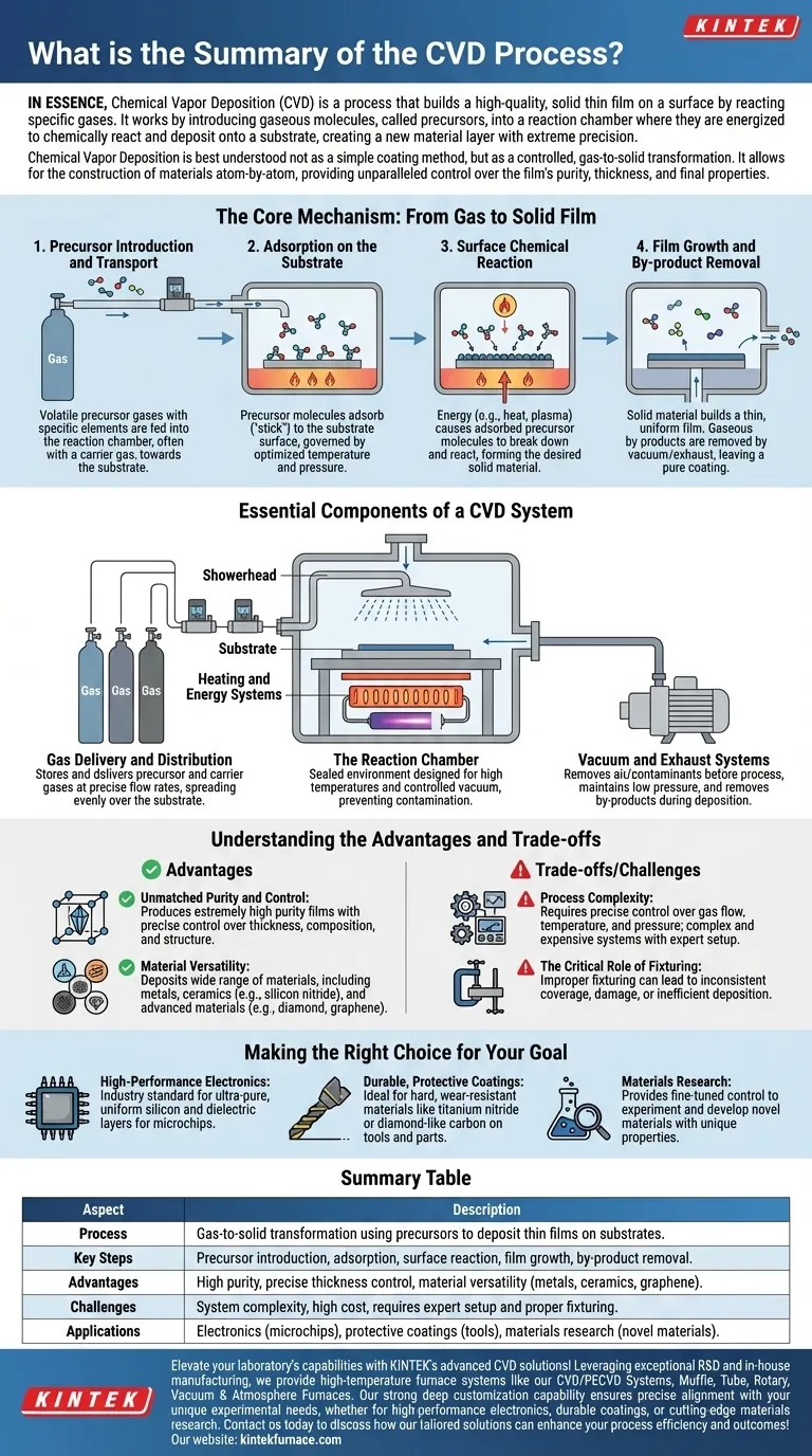
In essence, Chemical Vapor Deposition (CVD) is a process that builds a high-quality, solid thin film on a surface by reacting specific gases. It works by introducing gaseous molecules, called precursors, into a reaction chamber where they are energized to chemically react and deposit onto a substrate, creating a new material layer with extreme precision.
Chemical Vapor Deposition is best understood not as a simple coating method, but as a controlled, gas-to-solid transformation. It allows for the construction of materials atom-by-atom, providing unparalleled control over the film's purity, thickness, and final properties.
The Core Mechanism: From Gas to Solid Film
The CVD process can be broken down into a sequence of carefully controlled physical and chemical events. Each step is critical for achieving a uniform and high-purity final product.
### 1. Precursor Introduction and Transport
The process begins by feeding one or more volatile precursor gases into the reaction chamber. These gases contain the specific elements that will form the final film. A carrier gas often helps transport these precursors toward the target surface, known as the substrate.
### 2. Adsorption on the Substrate
Once near the substrate, the precursor molecules adsorb, or "stick," to its surface. This step is governed by the chamber's temperature and pressure, which are optimized to ensure the molecules attach correctly without re-evaporating.
### 3. Surface Chemical Reaction
This is the heart of the CVD process. With energy applied—typically in the form of heat—the adsorbed precursor molecules break down and chemically react. This reaction forms the desired solid material directly on the substrate's surface.
### 4. Film Growth and By-product Removal
The solid material from the reaction builds up layer by layer, forming a thin, uniform film. Gaseous by-products from the reaction desorb from the surface and are carried away by a vacuum or exhaust system, leaving behind a pure and solid coating.
Essential Components of a CVD System
A successful CVD process relies on a sophisticated system where every parameter is precisely managed.
### The Reaction Chamber
This is the sealed environment where the deposition occurs. It is designed to withstand high temperatures and maintain a controlled vacuum to prevent contamination.
### Gas Delivery and Distribution
This system stores the precursor and carrier gases and delivers them into the chamber at precise flow rates. A "showerhead" or similar distribution mechanism ensures the gases spread evenly over the substrate.
### Heating and Energy Systems
A heating system raises the substrate to the temperature required for the chemical reaction to occur. In some variations, like Plasma-Enhanced CVD (PECVD), a plasma is used to provide the energy, allowing the process to run at lower temperatures.
### Vacuum and Exhaust Systems
A vacuum pump is used to remove air and contaminants from the chamber before the process begins. During deposition, it maintains the precise low pressure needed and removes the gaseous by-products.
Understanding the Advantages and Trade-offs
While powerful, CVD is a specialized process with distinct advantages and practical considerations.
### Advantage: Unmatched Purity and Control
Because the process builds the film from gaseous precursors in a controlled vacuum, it can produce films of extremely high purity. It also offers precise control over thickness, composition, and crystalline structure.
### Advantage: Material Versatility
CVD is not limited to one type of material. It can be used to deposit a wide range of materials, including metals, ceramics (like silicon nitride), and even advanced materials like diamond and graphene.
### Challenge: Process Complexity
The need for precise control over gas flow, temperature, and pressure makes CVD systems complex and expensive. The process requires significant expertise to set up and maintain.
### Challenge: The Critical Role of Fixturing
The quality of the final coating is highly dependent on how the substrate is held. Improper fixturing can lead to inconsistent coverage, damage to the part, or inefficient deposition, compromising the entire process.
Making the Right Choice for Your Goal
The decision to use CVD depends entirely on the desired outcome for your material.
- If your primary focus is high-performance electronics: CVD is the industry standard for creating the ultra-pure, uniform silicon and dielectric layers essential for microchips.
- If your primary focus is durable, protective coatings: CVD is ideal for depositing hard, wear-resistant materials like titanium nitride or diamond-like carbon on tools and mechanical parts.
- If your primary focus is materials research: CVD provides the fine-tuned control needed to experiment with and develop novel materials with unique compositions and properties.
By mastering the transformation of gas into a solid, CVD empowers engineers and scientists to build materials from the ground up.
Summary Table:
| Aspect | Description |
|---|---|
| Process | Gas-to-solid transformation using precursors to deposit thin films on substrates. |
| Key Steps | Precursor introduction, adsorption, surface reaction, film growth, by-product removal. |
| Advantages | High purity, precise thickness control, material versatility (metals, ceramics, graphene). |
| Challenges | System complexity, high cost, requires expert setup and proper fixturing. |
| Applications | Electronics (microchips), protective coatings (tools), materials research (novel materials). |
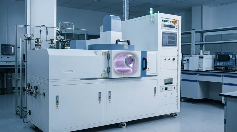
Elevate your laboratory's capabilities with KINTEK's advanced CVD solutions! Leveraging exceptional R&D and in-house manufacturing, we provide high-temperature furnace systems like our CVD/PECVD Systems, Muffle, Tube, Rotary, Vacuum & Atmosphere Furnaces. Our strong deep customization capability ensures precise alignment with your unique experimental needs, whether for high-performance electronics, durable coatings, or cutting-edge materials research. Contact us today to discuss how our tailored solutions can enhance your process efficiency and outcomes!
Visual Guide
Related Products
- HFCVD Machine System Equipment for Drawing Die Nano Diamond Coating
- Cylindrical Resonator MPCVD Machine System for Lab Diamond Growth
- Custom Made Versatile CVD Tube Furnace Chemical Vapor Deposition CVD Equipment Machine
- 915MHz MPCVD Diamond Machine Microwave Plasma Chemical Vapor Deposition System Reactor
- RF PECVD System Radio Frequency Plasma Enhanced Chemical Vapor Deposition
People Also Ask
- What role does Chemical Vapor Deposition (CVD) equipment play in the surface coating of carbon fibers for composites?
- What is Hot-filament Chemical Vapor Deposition (HFCVD)? Achieve High-Quality Thin Films with Precision Control
- What are the equipment for chemical vapor deposition? A Guide to the 5 Essential Components
- What core function does CVD equipment serve in h-BN anti-corrosion? Master Precision Synthesis for High-Performance Films
- How can customers maximize the quality of CVD coatings? Master Pre-Coating Prep for Superior Results