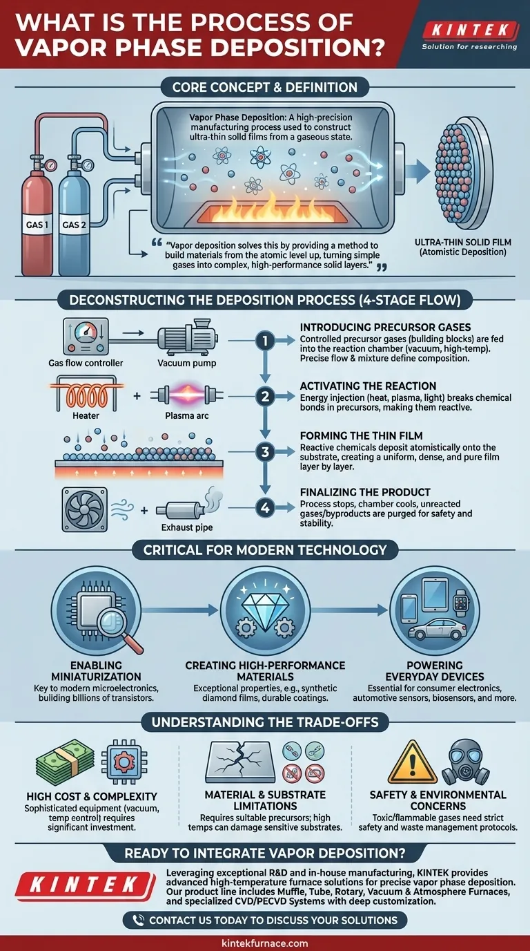
In essence, vapor phase deposition is a high-precision manufacturing process used to construct ultra-thin solid films from a gaseous state. It involves a controlled chemical reaction where volatile compounds (gases) are introduced into a chamber, react, and then deposit onto a target surface, building a new material one layer of atoms at a time. This method is fundamental to creating the high-performance components found in most modern electronics.
The core challenge in advanced manufacturing is not just shaping materials, but creating them with specific, engineered properties. Vapor deposition solves this by providing a method to build materials from the atomic level up, turning simple gases into complex, high-performance solid layers.
Deconstructing the Deposition Process
To understand vapor phase deposition, it's best to view it as a four-stage, highly controlled construction project happening on a microscopic scale. The most common method is known as Chemical Vapor Deposition (CVD).
The Core Principle: From Gas to Solid
The entire process is built on a simple idea: certain elements can be transported as a gas (a "precursor") and then converted into a solid through a chemical reaction.
By controlling the conditions of that reaction, we can control exactly how and where the solid material forms, allowing for the creation of extremely pure and uniform films.
Step 1: Introducing Precursor Gases
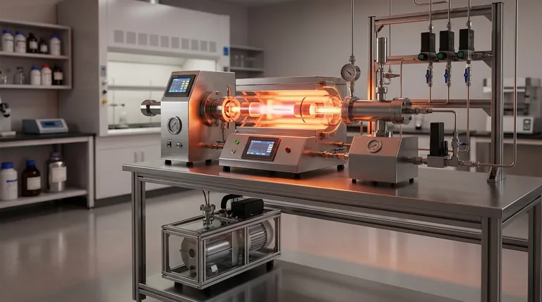
The process begins by feeding specific gaseous compounds into a reaction chamber, typically a high-temperature furnace under vacuum.
These precursor gases are the building blocks of the final film. Their flow rates and mixture ratios are precisely controlled, as this determines the chemistry and composition of the material being created.
Step 2: Activating the Reaction with Energy
For the precursors to react, they need an injection of energy. Most commonly, this is achieved by heating the chamber and the substrate to very high temperatures.
In other variations, this energy can be supplied by plasma (an ionized gas), as is the case when creating synthetic diamonds, or even concentrated light. This energy breaks the chemical bonds in the precursor gases, making them available to form new solids.
Step 3: Forming the Thin Film
Once activated, the precursor chemicals react near the heated substrate—the target material being coated.
The product of this reaction is a non-volatile solid that deposits atomistically (atom by atom) onto the substrate's surface. This slow, controlled growth is what ensures the film is uniform, dense, and pure.
Step 4: Finalizing the Product
After the film has grown to the desired thickness, the process is stopped. The chamber is cooled, and any unreacted precursor gases and byproducts are purged from the system.
This final step is critical to prevent unwanted further deposition and to safely handle the often volatile gases used in the process.
Why This Process Is Critical for Modern Technology
Vapor deposition is not an academic exercise; it is a foundational pillar of the high-tech world, enabling the creation of devices we use every day.
Enabling Miniaturization
The ability to deposit perfect, ultra-thin layers is the key to modern microelectronics. The processors in your smartphone, for instance, contain billions of transistors built from layers of materials created through deposition.
Creating High-Performance Materials
This process can create materials with exceptional properties. A prime example is the deposition of synthetic diamond films, which are incredibly hard and thermally conductive, used for durable coatings and advanced electronics.
Powering Everyday Devices
From the sensors in your car's engine to the components in your smartwatch, vapor deposition is essential. It's used to create films for:
- Consumer electronics (smartphones, wearables)
- Automotive sensors and electronics
- Biosensors for medical diagnostics
- Smart utility meters and HVAC sensors
Understanding the Trade-offs
While powerful, vapor phase deposition is a complex and resource-intensive technique with inherent challenges.
High Cost and Complexity
Deposition systems, like CVD furnaces, are sophisticated and expensive pieces of equipment. They require vacuum systems, precise gas handling, and advanced temperature control, making the initial investment significant.
Material and Substrate Limitations
The process relies on having suitable volatile precursors, which don't exist for all materials. Furthermore, the high temperatures involved can damage or destroy sensitive substrates, limiting which materials can be coated.
Safety and Environmental Concerns
The precursor gases used are often toxic, flammable, or corrosive. This necessitates strict safety protocols for handling and storage, as well as systems to manage hazardous waste byproducts.
Applying This to Your Goal
Understanding vapor deposition is about recognizing it as a tool for atomic-level construction. How you apply it depends on your objective.
- If your primary focus is material science: This process is your key to creating novel, high-purity films with engineered properties that are impossible to achieve through conventional means.
- If your primary focus is electronics manufacturing: This is the industry-standard method for building the microscopic, multi-layered structures that form the basis of all modern semiconductor devices.
- If your primary focus is process engineering: Success in deposition is a game of precision; mastering it requires absolute control over temperature, pressure, and gas flow dynamics within the reaction chamber.
Ultimately, vapor phase deposition is the invisible engine that translates the chemistry of gases into the tangible, high-performance solid materials that define our technological age.
Summary Table:
| Stage | Key Action | Outcome |
|---|---|---|
| 1. Precursor Introduction | Controlled gases enter a vacuum chamber. | Building blocks are in place for the reaction. |
| 2. Reaction Activation | Energy (heat, plasma) breaks chemical bonds. | Precursor gases become reactive. |
| 3. Film Formation | Reactive gases deposit atoms onto a substrate. | A uniform, high-purity thin film grows layer by layer. |
| 4. Finalization | Chamber is cooled and byproducts are purged. | A stable, finished film with precise properties is created. |
Ready to Integrate Vapor Deposition into Your Lab?
Leveraging exceptional R&D and in-house manufacturing, KINTEK provides diverse laboratories with advanced high-temperature furnace solutions for precise vapor phase deposition. Our product line—including Muffle, Tube, and Rotary Furnaces, Vacuum & Atmosphere Furnaces, and specialized CVD/PECVD Systems—is complemented by strong deep customization capabilities to precisely meet your unique experimental requirements, whether for material science, electronics manufacturing, or process engineering.
Contact us today to discuss how our solutions can help you build the next generation of high-performance materials and devices. Get in Touch
Visual Guide
Related Products
- RF PECVD System Radio Frequency Plasma Enhanced Chemical Vapor Deposition
- Custom Made Versatile CVD Tube Furnace Chemical Vapor Deposition CVD Equipment Machine
- Multi Heating Zones CVD Tube Furnace Machine for Chemical Vapor Deposition Equipment
- 915MHz MPCVD Diamond Machine Microwave Plasma Chemical Vapor Deposition System Reactor
- MPCVD Machine System Reactor Bell-jar Resonator for Lab and Diamond Growth
People Also Ask
- What are the system specifications of the PECVD system? Unlock Precision Thin-Film Deposition
- What are the limitations of PECVD? Overcome Process Control and Cost Challenges
- What is PECVD specification? A Guide to Choosing the Right System for Your Lab
- What are the applications of plasma enhanced chemical vapor deposition? Key Uses in Electronics, Optics & Materials
- What is RF in PECVD? A Critical Control for Plasma Deposition


