From the smartphone in your pocket to advanced optical systems, Plasma-Enhanced Chemical Vapor Deposition (PECVD) is a cornerstone technology for creating critical thin films. Its primary applications are in semiconductor manufacturing for depositing insulators, protective passivation layers, and hard masks for patterning circuits. Beyond microchips, PECVD is vital for producing high-performance optical coatings, anti-reflective layers, and functional components within Micro-Electro-Mechanical Systems (MEMS).
The fundamental advantage of PECVD is its ability to deposit high-quality, durable thin films at low temperatures. This single characteristic makes it possible to enhance heat-sensitive substrates like modern microchips and flexible electronics, a feat that is often impossible with traditional high-temperature methods.
Why PECVD Dominates in Advanced Manufacturing
The widespread adoption of PECVD is not accidental. It solves critical manufacturing challenges that older technologies like traditional Chemical Vapor Deposition (CVD) cannot. The core difference is how it supplies the energy needed for the chemical reaction.
The Low-Temperature Advantage
Traditional CVD requires very high temperatures (often >600°C) to break down precursor gases and deposit a film. This heat would destroy the intricate, multi-layered circuits already present on a modern silicon wafer.
PECVD sidesteps this issue by creating a plasma, an energized state of gas. The energy from the plasma, rather than extreme heat, drives the chemical reactions. This allows for deposition at much lower temperatures (typically 200-400°C), preserving the delicate structures underneath.
Unmatched Film Quality and Uniformity
The plasma environment enables the growth of films that are exceptionally dense and uniform across the entire substrate. This process results in fewer pinholes or defects.
Furthermore, PECVD films exhibit significantly less internal stress, making them much less prone to cracking. This ensures higher device reliability and longevity, which is non-negotiable for electronics.
Superior Adhesion and Coverage
The energized particles within the plasma also improve the adhesion of the deposited film to the substrate. The film sticks better and is more durable.
This process is also excellent at coating complex, non-flat surfaces, ensuring a consistent layer even over the microscopic topography of a microchip.
The Power of Tunable Properties
One of PECVD's most powerful features is the ability for engineers to precisely control the final film's characteristics. By adjusting process variables like gas composition, pressure, and plasma power, specific properties can be "dialed in."
Dialing in Optical Performance
For optical applications, the refractive index is a critical property. PECVD allows for its precise manipulation to create sophisticated anti-reflective coatings on lenses, sunglasses, and optical sensors. This control is essential for building complex optical filters and data storage systems.
Controlling Mechanical and Electrical Characteristics
In microelectronics, the goal is often to create a perfect insulator (a dielectric layer) or a hard, protective coating. With PECVD, engineers can fine-tune a film's dielectric constant, hardness, and chemical resistance to meet the exact electrical and mechanical demands of the device.
Understanding the Trade-offs and Process Realities
While powerful, PECVD is not a perfect solution for every scenario. Acknowledging its operational realities is key to successful implementation.
Chemical Contamination Risks
Many PECVD processes use precursor gases containing hydrogen (e.g., silane, SiH₄). Some of this hydrogen can become incorporated into the deposited film, which can subtly alter its electrical or optical properties. This is a well-understood variable that engineers must manage.
Potential for Plasma-Induced Damage
The high-energy environment of the plasma, while beneficial, can sometimes cause minor damage to the substrate surface. Process engineers work carefully to balance deposition speed and quality against the risk of this damage, optimizing the plasma conditions for each specific application.
Cost and Throughput Dynamics
The initial capital investment for PECVD equipment is significant. However, its cost-effectiveness emerges at scale. The process boasts high deposition rates—in some cases over 100 times faster than traditional CVD—and lower energy consumption per substrate, leading to higher throughput and reduced long-term operational costs.
Making the Right Choice for Your Goal
When evaluating thin-film deposition, PECVD's strengths align with specific engineering priorities.
- If your primary focus is protecting sensitive electronic components: PECVD is the superior choice for depositing high-quality passivation or dielectric layers without damaging underlying circuitry.
- If your primary focus is creating high-performance optical coatings: PECVD offers the precise control over refractive index and thickness needed to build complex anti-reflective and filter stacks.
- If your primary focus is rapid production and cost-efficiency at scale: PECVD's high deposition rates and lower energy use per substrate make it a highly effective solution for high-volume manufacturing.
Ultimately, understanding PECVD's low-temperature capabilities empowers you to build more advanced and reliable devices.
Summary Table:
| Key Feature | Benefit | Primary Application |
|---|---|---|
| Low-Temperature Deposition | Protects heat-sensitive components | Semiconductors, Flexible Electronics |
| Tunable Film Properties | Precise control of optical & electrical traits | Optical Coatings, MEMS |
| High Deposition Rate & Uniformity | Scalable production with fewer defects | High-Volume Manufacturing |
Ready to integrate PECVD's precision into your R&D or production line?
KINTEK's advanced high-temperature furnace solutions, including our CVD/PECVD Systems, are engineered for excellence. Leveraging exceptional R&D and in-house manufacturing, we provide diverse laboratories with the tools for innovation. Our strong deep customization capability ensures your unique experimental requirements for thin-film deposition are met precisely.
Contact our experts today to discuss how we can empower your next project.
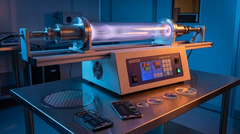
Visual Guide

Related Products
- Slide PECVD Tube Furnace with Liquid Gasifier PECVD Machine
- RF PECVD System Radio Frequency Plasma Enhanced Chemical Vapor Deposition
- Inclined Rotary Plasma Enhanced Chemical Deposition PECVD Tube Furnace Machine
- Inclined Rotary Plasma Enhanced Chemical Deposition PECVD Tube Furnace Machine
- Multi Heating Zones CVD Tube Furnace Machine for Chemical Vapor Deposition Equipment
People Also Ask
- What are the advantages of using a tube furnace CVD system for Cu(111)/graphene? Superior Scalability and Quality
- In which industries is the tube furnace commonly used? Essential for Materials Science, Energy, and More
- How does a hydrogen reduction environment in an industrial tube furnace facilitate gold-copper alloy microspheres?
- What is plasma in the context of PECVD? Unlock Low-Temperature Thin Film Deposition
- What role does a Tube Furnace play in the CVD growth of carbon nanotubes? Achieve High-Purity CNT Synthesis


