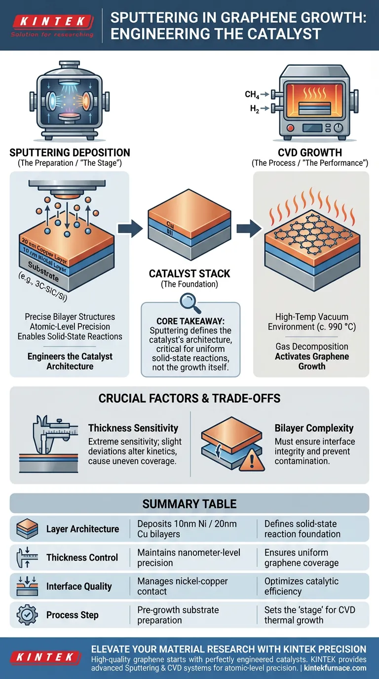
In the context of catalytic epitaxial growth, the primary function of a sputtering deposition system is to engineer the precise metal catalyst layers required to initiate the reaction.
Specifically, it is used to deposit exact bilayer structures—such as a 10 nm nickel layer followed by a 20 nm copper layer—onto substrates like 3C-SiC/Si, providing the essential foundation for solid-state source reactions.
Core Takeaway Sputtering is not the mechanism of graphene growth itself, but the critical preparation step that defines the architecture of the catalyst. By strictly controlling the thickness and composition of metal films (like nickel and copper), it enables the uniform solid-state reactions necessary to achieve high-quality graphene coverage.
The Role of Sputtering in Substrate Preparation
Creating the Catalytic Stack
The sputtering system is responsible for depositing the specific metal layers that act as catalysts.
In this process, it applies a bilayer structure to the substrate. The primary reference highlights a specific configuration: a 10 nm layer of nickel followed by a 20 nm layer of copper.
Achieving Atomic-Level Precision
The success of epitaxial growth hinges on the uniformity of these metal layers.
The sputtering system must provide precise control over the thin-film thickness. This precision ensures that the catalyst is distributed evenly across the substrate, preventing irregularities that could disrupt the graphene structure.
Enabling Solid-State Reactions
Unlike methods that rely solely on gaseous precursors, this approach utilizes solid-state source reactions.
The metal layers deposited by the sputtering system facilitate these reactions. They act as the medium through which carbon atoms interact and rearrange, ultimately forming the graphene lattice.
Distinguishing Sputtering from CVD
Sputtering vs. Growth Environment
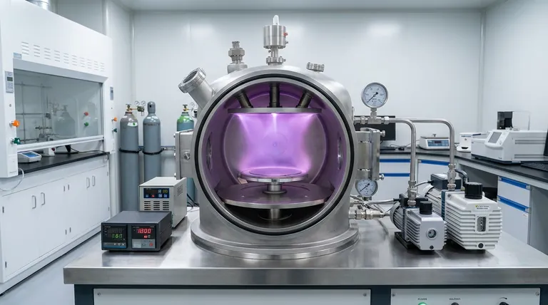
It is vital to distinguish the sputtering phase from the chemical vapor deposition (CVD) phase.
As noted in the supplementary references, a CVD system controls the high-temperature vacuum environment and gas flow (such as methane and hydrogen). The CVD system is where the growth occurs thermodynamically.
The Foundation vs. The Process
The sputtering system builds the "stage," while the CVD system directs the "performance."
Sputtering establishes the metal substrate properties (the copper/nickel stack). The CVD system then utilizes heat (around 990 °C) and gas decomposition to activate the growth of graphene upon that sputtered foundation.
Understanding the Trade-offs
Thickness Sensitivity
The primary challenge in using sputtering for this application is the extreme sensitivity of the solid-state reaction to film thickness.
If the nickel or copper layers deviate even slightly from the target (e.g., 10 nm/20 nm), the reaction kinetics change. This can lead to uneven coverage or failure to achieve a continuous single layer.
Complexity of Bilayers
Managing a bilayer deposition adds complexity compared to using a single metal foil.
You must ensure not only the correct thickness of each layer but also the integrity of the interface between the nickel and copper. Any contamination between these sputtered layers can degrade the catalytic performance.
Making the Right Choice for Your Goal
To maximize the effectiveness of your sputtering deposition system in this process, consider your specific objectives:
- If your primary focus is Uniformity: Ensure your sputtering system is calibrated to maintain thickness consistency across the entire wafer, as variations will directly mirror in the graphene coverage.
- If your primary focus is Reaction Kinetics: Adhere strictly to the demonstrated bilayer ratios (such as the 10 nm Ni / 20 nm Cu stack) to replicate successful solid-state source reactions.
- If your primary focus is Scalability: Verify that your sputtering process can reproduce these nanometer-scale thicknesses rapidly without introducing defects into the metal lattice.
The quality of your graphene is predetermined by the precision of your metal catalyst deposition.
Summary Table:
| Feature | Role in Graphene Growth | Impact on Result |
|---|---|---|
| Layer Architecture | Deposits 10nm Ni / 20nm Cu bilayers | Defines the solid-state reaction foundation |
| Thickness Control | Maintains nanometer-level precision | Ensures uniform graphene coverage |
| Interface Quality | Manages nickel-copper contact | Optimizes catalytic efficiency |
| Process Step | Pre-growth substrate preparation | Sets the 'stage' for CVD thermal growth |
Elevate Your Material Research with KINTEK Precision
High-quality graphene starts with a perfectly engineered catalyst layer. Backed by expert R&D and world-class manufacturing, KINTEK provides the advanced Sputtering systems and Lab High-Temp Furnaces (including Muffle, Tube, Vacuum, and CVD systems) necessary to achieve atomic-level precision. Whether you are developing complex bilayers or scaling up solid-state reactions, our customizable equipment is designed to meet your unique laboratory needs.
Ready to optimize your thin-film deposition and epitaxial growth?
Contact our experts today to find the perfect solution for your research goals.
Visual Guide
References
- Aiswarya Pradeepkumar, Francesca Iacopi. Epitaxial graphene growth on cubic silicon carbide on silicon with high temperature neutron reflectometry: an <i>operando</i> study. DOI: 10.1039/d3ra08289j
This article is also based on technical information from Kintek Furnace Knowledge Base .
Related Products
- HFCVD Machine System Equipment for Drawing Die Nano Diamond Coating
- RF PECVD System Radio Frequency Plasma Enhanced Chemical Vapor Deposition
- Cylindrical Resonator MPCVD Machine System for Lab Diamond Growth
- Custom Made Versatile CVD Tube Furnace Chemical Vapor Deposition CVD Equipment Machine
- 915MHz MPCVD Diamond Machine Microwave Plasma Chemical Vapor Deposition System Reactor
People Also Ask
- What core function does CVD equipment serve in h-BN anti-corrosion? Master Precision Synthesis for High-Performance Films
- What is the significance of the vacuum pressure control system in the CVD coating process for powders?
- What is Hot-filament Chemical Vapor Deposition (HFCVD)? Achieve High-Quality Thin Films with Precision Control
- What materials are commonly used in CVD coating systems? Explore Key Materials for Superior Coatings
- How can customers maximize the quality of CVD coatings? Master Pre-Coating Prep for Superior Results


