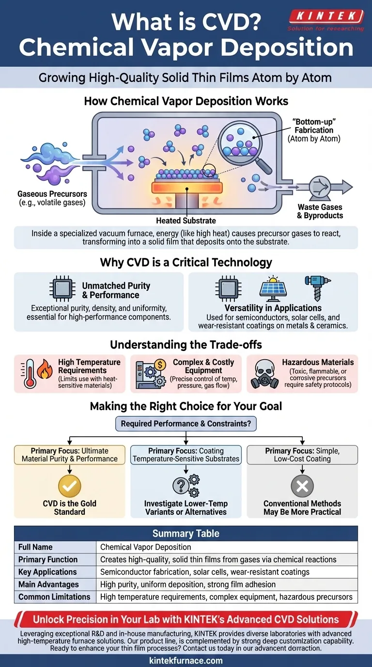
At its core, CVD stands for Chemical Vapor Deposition. It is a sophisticated manufacturing process used to create high-quality, solid thin films on a surface by transforming gases into a solid material through controlled chemical reactions.
The crucial insight is that CVD isn't merely a coating method; it's a "bottom-up" fabrication technique that grows a new, highly pure, and uniform solid layer atom by atom. This precision is why it is foundational to the entire semiconductor and advanced materials industry.
How Chemical Vapor Deposition Works
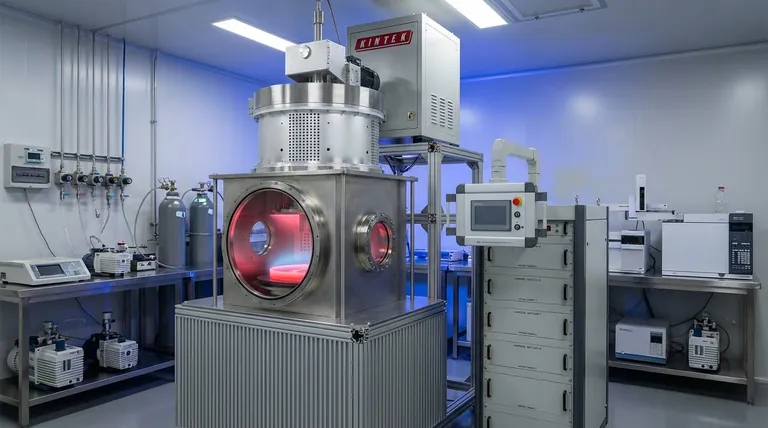
CVD is a highly controlled process that takes place inside a specialized piece of equipment, typically a high-temperature furnace operating under a vacuum. The entire process can be broken down into a few key stages.
The Role of Gaseous Precursors
The process begins with one or more volatile gases known as precursors. These gases contain the chemical elements that will make up the final solid film.
These precursors are precisely injected into a reaction chamber that contains the object to be coated, known as the substrate.
The Reaction Chamber and Deposition
Inside the chamber, energy—most often high heat—is applied. This energy causes the precursor gases to become highly reactive.
The energized gases then decompose or react with each other on the surface of the heated substrate. This chemical reaction is the "CVD" process itself.
Forming the Solid Thin Film
As the chemical reaction occurs, the gaseous precursors are converted into a solid material that deposits onto the substrate, forming a thin, uniform, and tightly bonded film.
The waste gases and byproducts of the reaction are then pumped out of the chamber, leaving behind only the substrate with its newly formed layer.
Why CVD is a Critical Technology
The precision and quality of the films produced by CVD make it an indispensable process in many high-tech fields. It is not just about applying a coating, but about creating a new, functional layer of material.
Unmatched Purity and Performance
CVD produces films that are exceptionally pure, dense, and uniform across the entire substrate. This level of quality is essential for creating high-performance components.
Versatility in Applications
This technique is used to deposit a wide range of materials, including metals, ceramics, and semiconductors.
Its primary applications are in industries where material performance is paramount, such as semiconductor fabrication (for creating microchips), solar cell production, and the creation of hard, wear-resistant coatings for cutting tools.
Understanding the Trade-offs
While powerful, CVD is not a universal solution. Its effectiveness comes with specific requirements and limitations that are important to understand.
High Temperature Requirements
Traditional CVD processes often require very high temperatures, which can damage or warp certain substrate materials. This limits its use with plastics or other low-melting-point materials.
Complexity of Equipment
A CVD furnace is a complex and expensive piece of equipment. It requires precise control over temperature, pressure, and gas flow, making both the initial investment and ongoing operation costly.
Hazardous Materials
The precursor gases used in CVD can be highly toxic, flammable, or corrosive. This necessitates sophisticated safety protocols, handling systems, and exhaust management, adding to the overall complexity.
Making the Right Choice for Your Goal
Deciding whether CVD is appropriate depends entirely on the required performance and constraints of your project.
- If your primary focus is ultimate material purity and performance: CVD is the gold standard for creating the highest-quality thin films required for advanced electronics and optical components.
- If your primary focus is coating temperature-sensitive substrates: You must investigate specialized, lower-temperature CVD variants or consider alternative deposition methods entirely.
- If your primary focus is simple, low-cost coating: The high cost and complexity of CVD are likely unnecessary, and more conventional methods would be more practical.
Ultimately, Chemical Vapor Deposition is the enabling technology behind many of the high-performance materials that define our modern world.
Summary Table:
| Aspect | Details |
|---|---|
| Full Name | Chemical Vapor Deposition |
| Primary Function | Creates high-quality, solid thin films by converting gases into solids via chemical reactions |
| Key Applications | Semiconductor fabrication, solar cells, wear-resistant coatings |
| Main Advantages | High purity, uniform deposition, strong film adhesion |
| Common Limitations | High temperature requirements, complex equipment, hazardous precursors |
Unlock Precision in Your Lab with KINTEK's Advanced CVD Solutions
Leveraging exceptional R&D and in-house manufacturing, KINTEK provides diverse laboratories with advanced high-temperature furnace solutions. Our product line, including CVD/PECVD Systems, Muffle, Tube, Rotary Furnaces, and Vacuum & Atmosphere Furnaces, is complemented by strong deep customization capability to precisely meet your unique experimental requirements. Whether you're in semiconductor research, solar energy, or materials science, we deliver reliable, high-performance equipment tailored to your needs.
Ready to enhance your thin film processes? Contact us today to discuss how our CVD systems can drive your innovations forward!
Visual Guide
Related Products
- Custom Made Versatile CVD Tube Furnace Chemical Vapor Deposition CVD Equipment Machine
- Multi Heating Zones CVD Tube Furnace Machine for Chemical Vapor Deposition Equipment
- HFCVD Machine System Equipment for Drawing Die Nano Diamond Coating
- Split Chamber CVD Tube Furnace with Vacuum Station CVD Machine
- 915MHz MPCVD Diamond Machine Microwave Plasma Chemical Vapor Deposition System Reactor
People Also Ask
- What is the working principle of a CVD tube furnace? Achieve Precise Thin Film Deposition for Your Lab
- What customization options are available for CVD tube furnaces? Tailor Your System for Superior Material Synthesis
- How does CVD tube furnace sintering enhance graphene growth? Achieve Superior Crystallinity and High Electron Mobility
- Which industries and research fields benefit from CVD tube furnace sintering systems for 2D materials? Unlock Next-Gen Tech Innovations
- How might AI and machine learning enhance CVD tube furnace processes? Boost Quality, Speed, and Safety


