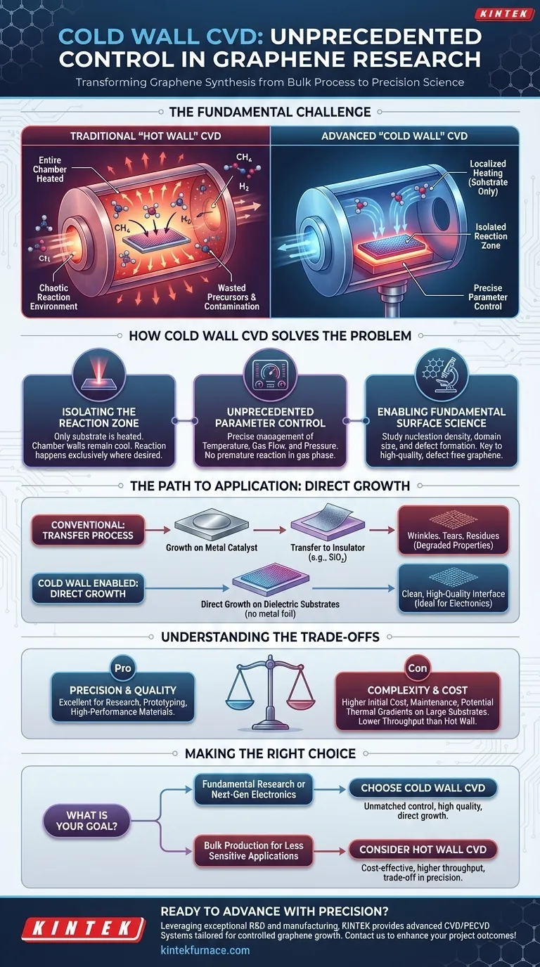
At its core, the significance of the cold wall Chemical Vapor Deposition (CVD) technique in graphene research is its ability to provide unprecedented control over the growth process. Unlike traditional methods where the entire chamber is heated, cold wall CVD isolates the reaction exclusively to the substrate surface, allowing researchers to precisely manipulate parameters like temperature, gas flow, and pressure. This transforms graphene synthesis from a bulk process into a controlled, surface-science experiment.
The central advantage of cold wall CVD is not just growing graphene, but understanding how it grows. By creating a highly controlled microenvironment at the substrate, the technique enables the fundamental research necessary to produce high-quality, defect-free graphene suitable for demanding electronic applications.
The Fundamental Challenge: Controlling Graphene Growth
The Basics of Chemical Vapor Deposition (CVD)
Chemical Vapor Deposition is the most common method for synthesizing large-area, high-quality graphene. In a typical process, a carbon-containing gas like methane (CH₄) is introduced into a chamber with a catalyst substrate, usually copper.
Gases like hydrogen (H₂) are also used to control the reaction and promote the orderly deposition of carbon atoms into the honeycomb lattice of graphene. The ratio of these gases is critical; too much hydrogen can corrode the newly formed graphene sheet.
The Problem with "Hot Wall" Reactors
In a traditional "hot wall" CVD system, the entire furnace or tube is heated to the reaction temperature. This lack of thermal precision means precursor gases can decompose and react in the gas phase or on the chamber walls, not just on the target substrate.
This leads to wasted precursors, potential contamination, and a lack of fine control over the nucleation (the initial formation of graphene islands) and subsequent growth. It is difficult to study the fundamental science when the reaction environment is so chaotic.
How Cold Wall CVD Solves the Control Problem
Isolating the Reaction Zone
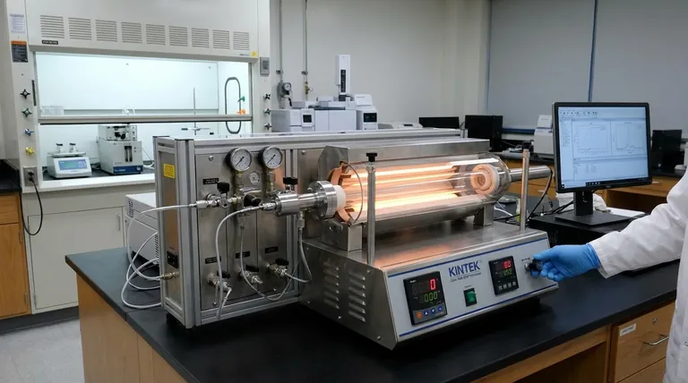
The defining feature of a cold wall CVD reactor is that only the substrate holder is actively heated, typically through resistive or inductive heating. The chamber walls remain cool.
This simple but powerful change ensures that the chemical reaction—the breakdown of methane and deposition of carbon—happens almost exclusively on the hot substrate surface where you want it.
Unprecedented Parameter Control
By confining the reaction to the substrate, researchers gain unprecedented control over the most sensitive process parameters. Gas flow rates and pressure can be managed precisely because the gases are not reacting prematurely in the heated volume of the chamber.
This allows for the systematic study of how each variable impacts the final material quality, moving graphene synthesis closer to the precision standards of the semiconductor industry.
Enabling Fundamental Surface Science
This level of control is invaluable for studying the surface-mediated science of how graphene forms. Researchers can use cold wall CVD to gain conclusive insights into nucleation density, domain size, and defect formation.
Understanding these fundamental mechanisms is the key to reliably producing large, single-crystalline domains of graphene, which is the holy grail for high-performance electronics.
Understanding the Trade-offs
System Complexity and Cost
Cold wall CVD systems are inherently more complex than simple hot wall tube furnaces. The localized heating, vacuum requirements, and precise gas handling systems contribute to higher initial cost and maintenance overhead.
Thermal Gradients
Heating only the substrate can create significant thermal gradients across the sample, especially on larger substrates. If not managed carefully, this can lead to non-uniform growth, where the quality of the graphene varies from the center to the edge of the wafer.
Throughput vs. Precision
Cold wall CVD is a tool optimized for precision and research. While excellent for developing new processes and fabricating high-quality material for prototypes, traditional hot wall systems may offer higher throughput for less demanding, bulk production scenarios.
The Path to Application: Direct Growth on Dielectrics
Avoiding the Damaging Transfer Process
For most electronic applications, graphene grown on a metal catalyst must be transferred to an insulating substrate, like silicon dioxide. This transfer process is notorious for introducing wrinkles, tears, and polymer residues that degrade graphene's exceptional electronic properties.
Direct Growth on Insulators
A key area of research, enabled by the control of advanced CVD systems, is the direct growth of graphene on dielectric substrates. Techniques like gaseous catalyst-assisted CVD, which can be implemented in a cold wall reactor, eliminate the need for a metal foil and the subsequent damaging transfer step.
This is a critical pathway for integrating graphene directly into semiconductor fabrication workflows, paving the way for its use in next-generation electronics and optoelectronics.
Making the Right Choice for Your Goal
Deciding on a synthesis method depends entirely on your end goal.
- If your primary focus is fundamental research: Cold wall CVD is the superior choice for its unmatched control over growth parameters, enabling you to study nucleation and growth mechanisms.
- If your primary focus is developing next-generation electronics: A cold wall system is critical for producing high-quality material and exploring advanced techniques like direct growth on dielectric substrates.
- If your primary focus is bulk production for less sensitive applications: A traditional hot wall reactor may provide a more cost-effective solution, accepting a trade-off in process control and ultimate material purity.
Ultimately, mastering the tool that provides the right level of control is the definitive step toward realizing the specific potential of graphene for your project.
Summary Table:
| Aspect | Description |
|---|---|
| Core Advantage | Isolates reaction to substrate for precise control over temperature, gas flow, and pressure. |
| Key Benefit | Enables fundamental study of nucleation and growth, leading to high-quality, defect-free graphene. |
| Ideal For | Fundamental research and next-generation electronics development, such as direct growth on dielectrics. |
| Trade-offs | Higher complexity and cost compared to hot wall systems; potential for thermal gradients on large substrates. |
Ready to advance your graphene research with precision? Leveraging exceptional R&D and in-house manufacturing, KINTEK provides diverse laboratories with advanced high-temperature furnace solutions, including CVD/PECVD Systems. Our strong deep customization capability ensures we meet your unique experimental requirements for controlled graphene growth. Contact us today to discuss how our tailored solutions can enhance your project outcomes!
Visual Guide
Related Products
- HFCVD Machine System Equipment for Drawing Die Nano Diamond Coating
- Custom Made Versatile CVD Tube Furnace Chemical Vapor Deposition CVD Equipment Machine
- Cylindrical Resonator MPCVD Machine System for Lab Diamond Growth
- MPCVD Machine System Reactor Bell-jar Resonator for Lab and Diamond Growth
- RF PECVD System Radio Frequency Plasma Enhanced Chemical Vapor Deposition
People Also Ask
- What are the equipment for chemical vapor deposition? A Guide to the 5 Essential Components
- What is the advantage of using a CVD system for coating turbine blades? Master Complex Geometries with Ease
- What is chemical vapor deposition (CVD) and its primary industrial application? Unlock Precision Thin Films for Electronics
- What is the function of high-purity Argon (Ar) gas during CVD? Optimize Your Thin Film Uniformity and Purity
- What is Hot-filament Chemical Vapor Deposition (HFCVD)? Achieve High-Quality Thin Films with Precision Control


