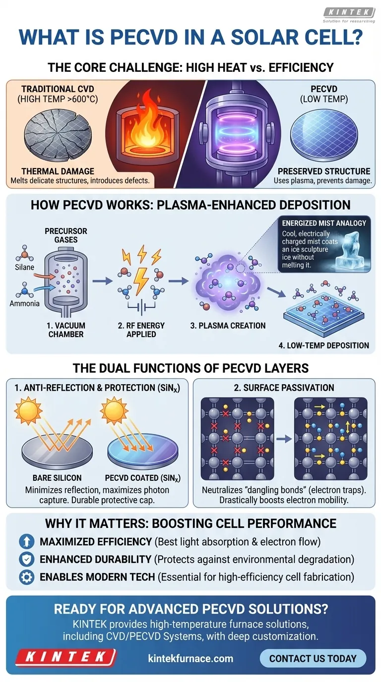
In solar cell manufacturing, PECVD is a critical process used to deposit extremely thin, high-performance films onto the cell's surface at low temperatures. This technique, Plasma-Enhanced Chemical Vapor Deposition, serves two primary functions: applying an anti-reflective coating to maximize sunlight absorption and "passivating" the silicon surface to improve its electrical efficiency. It accomplishes this without the high heat of other methods, which could damage the delicate solar cell structure.
The core challenge in making a high-efficiency solar cell is adding crucial performance-enhancing layers without damaging the underlying silicon. PECVD solves this by using an energized gas, or plasma, to deposit these films at low temperatures, simultaneously boosting light capture and electronic performance in a way that traditional high-temperature methods cannot.
The Core Problem: Why Temperature is the Enemy of Efficiency
The Need for Surface Layers
A bare silicon wafer is not an efficient solar cell. To perform well, it needs additional layers that help it capture more light and conduct electricity more effectively.
These layers must be incredibly thin, uniform, and possess specific optical and electrical properties.
The Damage Caused by High Heat
Traditional deposition methods, like thermal Chemical Vapor Deposition (CVD), require very high temperatures (often >600°C) to work.
Exposing a finished solar cell to such heat can introduce defects into the silicon crystal structure, effectively damaging the very components responsible for generating electricity. This thermal damage permanently reduces the cell's final efficiency.
How PECVD Works: Using Plasma Instead of Heat
The Role of Plasma
PECVD circumvents the need for high heat by using plasma. Inside a vacuum chamber, precursor gases (like silane and ammonia to create silicon nitride) are introduced.
Radio frequency (RF) energy is then applied, which ignites the gas into a plasma—an energized state of matter. This plasma has enough energy to break down the precursor gases into reactive molecules.
These reactive molecules then deposit onto the cooler solar cell surface, building up the desired thin film layer by layer.
The "Energized Mist" Analogy
Imagine trying to coat a delicate ice sculpture. Using hot steam (like traditional CVD) would melt and destroy it.
PECVD is like using a cool, electrically charged mist. The mist's particles are energized enough to stick and form a perfect coating, but the process is cool enough that it leaves the underlying ice sculpture completely unharmed.
The Two Primary Functions of PECVD in Solar Cells
Function 1: Anti-Reflection and Protection
The most common PECVD layer is silicon nitride (SiNx). The primary purpose of this layer is to act as an anti-reflective coating.
Bare silicon is shiny and reflects a significant portion of incoming sunlight. The precisely deposited SiNx layer has a refractive index that minimizes this reflection, allowing more photons (light) to enter the cell and generate power. This layer also provides a durable cap that protects the cell from moisture and contamination.
Function 2: Surface Passivation
This is the most critical function for electrical performance. The surface of a silicon crystal has "dangling bonds"—incomplete chemical bonds that act like traps for electrons.
When light creates an electron-hole pair, a trapped electron cannot contribute to the electrical current, effectively wasting its energy.
PECVD-deposited silicon nitride is rich in hydrogen. During the process, this hydrogen diffuses slightly into the silicon surface and "passivates" these dangling bonds, neutralizing the traps. This allows electrons to move freely, drastically improving charge carrier mobility and boosting the cell's overall conversion efficiency.
Understanding the Trade-offs
Equipment Complexity and Cost
PECVD systems are sophisticated vacuum chambers requiring RF power generators and precise gas control systems. This makes the equipment more complex and expensive to purchase and maintain than simpler high-temperature furnaces.
Process Control is Critical
The quality of the deposited film is highly sensitive to process parameters like pressure, gas flow rates, temperature, and plasma power. Any deviation can result in a sub-optimal film, negatively impacting the efficiency of the entire batch of solar cells.
Throughput vs. Necessity
While some manufacturing steps can be done faster, the gains from PECVD are so significant for modern high-efficiency cells that it is considered an essential, value-adding step. The trade-off in time is more than compensated for by the dramatic increase in final cell performance and monetary value.
Why This Matters for Solar Cell Efficiency
The decision to use PECVD is directly tied to the goal of producing commercially viable, high-performance solar panels. Its unique capabilities make it a cornerstone of the industry.
- If your primary focus is maximizing cell efficiency: PECVD is non-negotiable for its dual ability to provide both best-in-class anti-reflection and essential surface passivation.
- If your primary focus is creating durable, long-lasting panels: The dense silicon nitride film from PECVD provides excellent protection against environmental degradation.
- If your primary focus is understanding modern semiconductor fabrication: PECVD is a key example of the industry-wide shift toward low-temperature processes that enable more complex and delicate electronic devices.
Ultimately, PECVD is the enabling technology that transforms a functional silicon wafer into a high-efficiency solar cell ready for real-world power generation.
Summary Table:
| Key Aspect | PECVD's Role |
|---|---|
| Core Process | Deposits thin films using plasma at low temperatures |
| Primary Function | Anti-reflective coating and surface passivation |
| Temperature Advantage | Prevents thermal damage to delicate silicon wafers |
| Efficiency Impact | Maximizes light absorption and electron mobility |
| Common Material | Silicon Nitride (SiNx) with hydrogen for passivation |
Ready to enhance your solar cell manufacturing with advanced PECVD solutions? Leveraging exceptional R&D and in-house manufacturing, KINTEK provides diverse laboratories with advanced high-temperature furnace solutions. Our product line, including Muffle, Tube, Rotary Furnaces, Vacuum & Atmosphere Furnaces, and CVD/PECVD Systems, is complemented by our strong deep customization capability to precisely meet unique experimental requirements. Contact us today to discuss how our PECVD systems can boost your solar cell efficiency and durability!
Visual Guide
Related Products
- Slide PECVD Tube Furnace with Liquid Gasifier PECVD Machine
- RF PECVD System Radio Frequency Plasma Enhanced Chemical Vapor Deposition
- Inclined Rotary Plasma Enhanced Chemical Deposition PECVD Tube Furnace Machine
- Inclined Rotary Plasma Enhanced Chemical Deposition PECVD Tube Furnace Machine
- Multi Heating Zones CVD Tube Furnace Machine for Chemical Vapor Deposition Equipment
People Also Ask
- What are the main advantages of PECVD tube furnaces compared to CVD tube furnaces? Lower Temp, Faster Deposition, and More
- What role does a Tube Furnace play in the CVD growth of carbon nanotubes? Achieve High-Purity CNT Synthesis
- What are the typical conditions for plasma-enhanced CVD processes? Achieve Low-Temperature Thin Film Deposition
- What plasma source is used in PE-CVD tube furnaces? Unlock Low-Temperature, High-Quality Deposition
- What is plasma in the context of PECVD? Unlock Low-Temperature Thin Film Deposition


