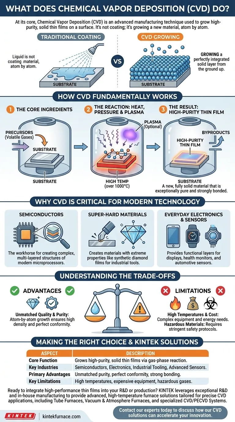
At its core, Chemical Vapor Deposition (CVD) is an advanced manufacturing technique used to grow high-purity, solid thin films on a surface. Instead of applying a liquid coating, CVD uses a chemical reaction in a gas phase to deposit a new material, layer by layer, directly onto a heated substrate, often on an atomic scale.
The crucial insight is that CVD is not simply about coating a surface; it's about growing a new, perfectly integrated solid layer from the ground up. This method allows for the creation of materials with exceptional purity and performance, which is why it is fundamental to the modern electronics and semiconductor industries.
How CVD Fundamentally Works
Chemical Vapor Deposition is a precise, highly controlled process that takes place inside a vacuum chamber. The basic principle can be broken down into a few key steps.
The Core Ingredients: A Substrate and Precursors
The process begins with a base material, called the substrate, which is the object to be coated. This substrate is placed inside a reaction chamber.
Then, one or more volatile gases, known as precursors, are introduced. These precursors contain the specific atoms needed to create the desired thin film.
The Reaction: Heat, Pressure, and Plasma
The chamber is heated to extremely high temperatures, sometimes over 1000°C. This high temperature provides the energy needed to trigger a chemical reaction.
This reaction causes the precursor gases to decompose on the hot substrate surface. The desired atoms from the gas bond to the substrate, forming a solid layer.
In some advanced CVD methods, a plasma (an energized gas) is used to facilitate the reaction at lower temperatures.
The Result: A High-Purity Thin Film
As the desired atoms deposit onto the substrate, they build up a dense, solid film. Any unwanted chemical byproducts from the reaction are simply vented out of the chamber.
The resulting film is not a simple paint or coating. It is a new, fully solid material that is exceptionally pure and strongly bonded to the underlying substrate.
Why CVD is Critical for Modern Technology
The ability to grow perfect, ultra-thin layers of material makes CVD an indispensable process for creating high-performance components across numerous industries.
The Foundation of Semiconductors
CVD is the workhorse of the semiconductor industry. It is used to deposit the various insulating, conducting, and semiconducting layers that form the microscopic transistors inside every computer chip.
Without CVD, manufacturing the complex, multi-layered structure of a modern microprocessor would be impossible.
Creating Super-Hard Materials
Specialized forms of CVD, such as microwave plasma CVD, are used to grow materials with extreme properties. This includes creating films of synthetic diamond.
These diamond films are used for durable industrial cutting tools, wear-resistant coatings, and advanced thermal management components in electronics.
Powering Everyday Electronics and Sensors
The impact of CVD is present in countless devices you use daily. It is used to create the functional layers in smartphone displays, wearable health monitors, automotive sensors, and smart utility meters.
These thin films provide the specific optical, electrical, or chemical properties that allow these devices to function.
Understanding the Trade-offs
While powerful, CVD is a specialized process with distinct advantages and limitations that make it suitable for specific, high-value applications.
Advantage: Unmatched Quality and Purity
The primary benefit of CVD is the ability to produce films of extremely high purity and density. Because the film is grown atom by atom, it conforms perfectly to even the most complex surface shapes.
Limitation: High Temperatures and Cost
Traditional CVD processes require very high temperatures, which can damage sensitive substrates like plastics.
Furthermore, the equipment—including high-vacuum chambers, precision gas handling systems, and high-temperature furnaces—is complex and expensive. This makes CVD a costly process best reserved for high-value manufacturing.
Limitation: Hazardous Materials
Many of the precursor gases used in CVD are toxic, flammable, or corrosive. Operating a CVD system requires stringent safety protocols and specialized facilities to handle these materials safely.
Making the Right Choice for Your Goal
Specifying or evaluating a CVD process depends entirely on the material properties you need to achieve for your specific application.
- If your primary focus is cutting-edge electronics: CVD is non-negotiable for depositing the ultra-pure silicon and dielectric films required for modern microprocessors.
- If your primary focus is extreme durability: Look to specialized CVD processes, like those used to grow synthetic diamond films for industrial tools or wear-resistant parts.
- If your primary focus is creating advanced sensors: CVD provides the means to deposit the sensitive, functional layers that enable biosensors, gas sensors, and pressure sensors in a wide array of devices.
Ultimately, chemical vapor deposition is the enabling technology that transforms raw gases into the high-performance solid materials that define our technological world.
Summary Table:
| Aspect | Description |
|---|---|
| Core Function | Grows high-purity, solid thin films on a substrate via a gas-phase chemical reaction. |
| Key Industries | Semiconductors, Electronics, Industrial Tooling, Advanced Sensors. |
| Primary Advantages | Unmatched film purity, perfect conformity to complex shapes, strong material bonding. |
| Key Limitations | High process temperatures, expensive equipment, handling of hazardous precursor gases. |
Ready to integrate high-performance thin films into your R&D or production?
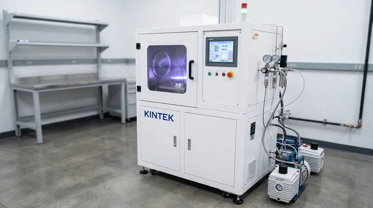
At KINTEK, we leverage our exceptional R&D and in-house manufacturing to provide advanced, high-temperature furnace solutions tailored for precise CVD applications. Whether you are developing next-generation semiconductors, super-hard coatings like diamond films, or sensitive sensor layers, our product line—including Tube Furnaces, Vacuum & Atmosphere Furnaces, and specialized CVD/PECVD Systems—is backed by strong deep customization capabilities to meet your unique experimental and production requirements.
Contact our experts today to discuss how our CVD solutions can accelerate your innovation.
Visual Guide
Related Products
- Custom Made Versatile CVD Tube Furnace Chemical Vapor Deposition CVD Equipment Machine
- MPCVD Machine System Reactor Bell-jar Resonator for Lab and Diamond Growth
- Multi Heating Zones CVD Tube Furnace Machine for Chemical Vapor Deposition Equipment
- 915MHz MPCVD Diamond Machine Microwave Plasma Chemical Vapor Deposition System Reactor
- Slide PECVD Tube Furnace with Liquid Gasifier PECVD Machine
People Also Ask
- What customization options are available for CVD tube furnaces? Tailor Your System for Superior Material Synthesis
- What are the key features of CVD tube furnaces for 2D material processing? Unlock Precision Synthesis for Superior Materials
- What improvements can be made to the bonding force of gate dielectric films using a CVD tube furnace? Enhance Adhesion for Reliable Devices
- What is a CVD tube furnace and what is its primary function? Discover Precision Thin-Film Deposition
- How might AI and machine learning enhance CVD tube furnace processes? Boost Quality, Speed, and Safety


