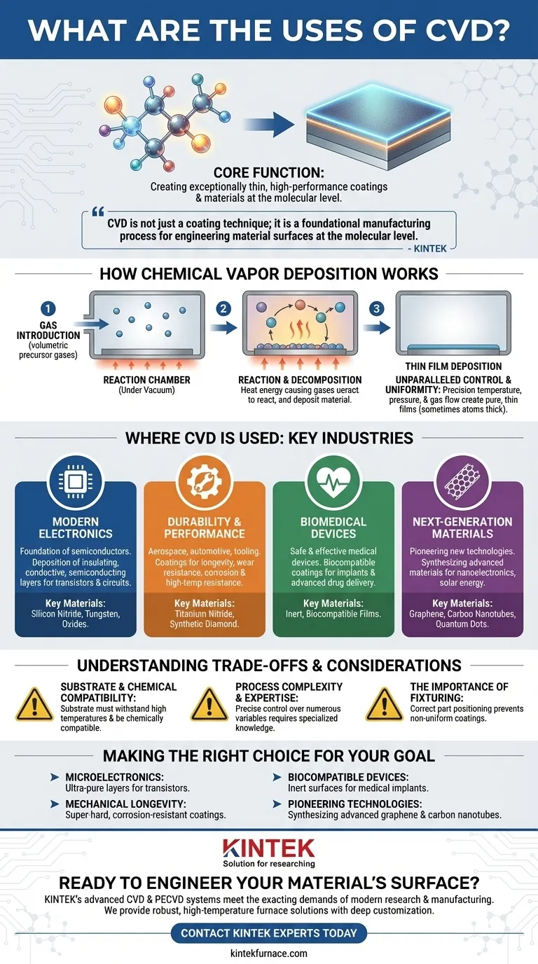
At its core, Chemical Vapor Deposition (CVD) is used to create exceptionally thin, high-performance coatings and materials on a substrate. This process is fundamental to manufacturing modern electronics like semiconductors, enhancing the durability of tools and components with protective layers, and producing advanced materials such as graphene and synthetic diamonds.
CVD is not just a coating technique; it is a foundational manufacturing process for engineering material surfaces at the molecular level. It allows us to build materials from the ground up, granting them specific electrical, mechanical, or biological properties that the base material lacks.
How Chemical Vapor Deposition Works
The Basic Principle: Building from Gas
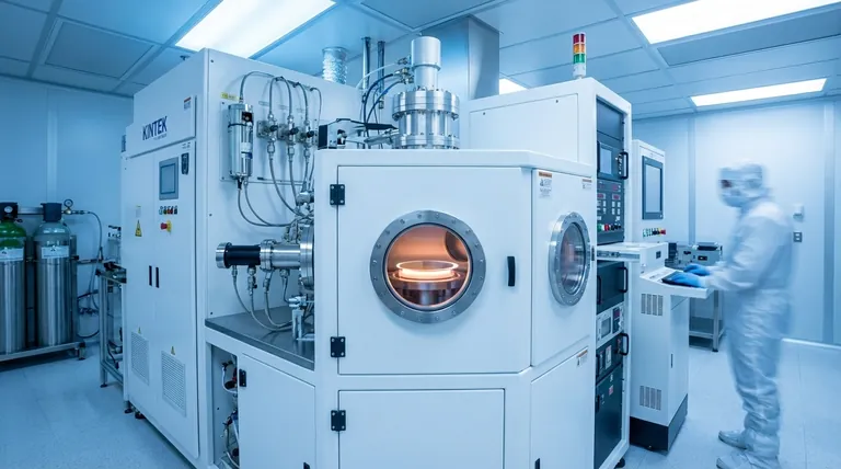
Chemical Vapor Deposition is a process where a substrate (the object to be coated) is placed in a reaction chamber, typically under vacuum.
Volatile precursor gases, which contain the atoms for the desired coating, are introduced into the chamber.
Heat or other energy sources cause these gases to react or decompose, depositing a solid, thin film of the new material onto the substrate's surface.
Unparalleled Control and Uniformity
The primary advantage of CVD is its precision. By carefully controlling temperature, pressure, and gas flow, the process can create coatings that are incredibly uniform, pure, and thin—sometimes only a few atoms thick.
This level of control is what makes CVD indispensable for applications where microscopic consistency is critical.
Where CVD is Used: A Breakdown of Key Industries
CVD is a versatile enabling technology that impacts nearly every advanced industry. Its applications are defined by the problem it solves: modifying a surface to achieve a new function.
The Foundation of Modern Electronics
The entire semiconductor industry is built upon CVD. It is used to deposit the ultra-thin layers of insulating, conductive, and semiconducting materials that form transistors and circuits on silicon wafers.
Materials like silicon nitride, tungsten, and various oxides are deposited with nanoscale precision to create the intricate architecture of microchips.
Enhancing Durability and Performance
In the aerospace, automotive, and tooling industries, CVD provides coatings that dramatically improve the longevity and performance of components.
By depositing films of materials like titanium nitride or synthetic diamond, CVD can make cutting tools incredibly hard and wear-resistant. It is also used to create coatings that make metals highly resistant to corrosion and high temperatures.
Revolutionizing Biomedical Devices
CVD is critical for making medical devices safe and effective inside the human body. It is used to apply biocompatible coatings to implants like artificial joints and dental implants.
These inert coatings prevent the body from rejecting the implant and can also be engineered to create advanced drug delivery systems with controlled-release properties.
Enabling Next-Generation Materials
CVD is the primary method for synthesizing many of the most promising advanced materials.
This includes two-dimensional materials like graphene, ultra-strong carbon nanotubes, and light-emitting quantum dots. These materials, built atom-by-atom with CVD, are at the heart of research in next-generation electronics, nanotechnology, and solar energy.
Understanding the Trade-offs and Considerations
While powerful, CVD is a sophisticated process that requires careful planning to be successful. It is not a simple "one-size-fits-all" solution.
Substrate and Chemical Compatibility
The chosen coating material must be chemically compatible with the substrate material. Furthermore, the substrate must be able to withstand the high temperatures often required by the CVD process.
Process Complexity and Expertise
Achieving a high-quality, uniform coating requires precise control over numerous variables, including temperature, pressure, gas chemistry, and flow rates. This demands significant process expertise and specialized equipment.
The Importance of Fixturing
How a part is held and positioned within the reaction chamber is critical. Poor fixture design can lead to non-uniform gas flow, resulting in inconsistent coating thickness and quality across the part's surface.
Making the Right Choice for Your Goal
CVD is a tool for fundamentally changing a material's properties. The best application depends entirely on your desired outcome.
- If your primary focus is creating microelectronics: CVD is non-negotiable for depositing the ultra-pure insulating and conductive layers that form transistors.
- If your primary focus is improving mechanical longevity: CVD is the ideal method for applying super-hard or corrosion-resistant coatings to extend the life of tools and components.
- If your primary focus is developing biocompatible devices: CVD provides the essential inert surfaces on medical implants to ensure they function safely within the body.
- If your primary focus is pioneering new technologies: CVD is the key manufacturing process for synthesizing advanced materials like graphene and carbon nanotubes.
Ultimately, Chemical Vapor Deposition is a cornerstone of modern material science, enabling the creation of products and technologies that would otherwise be impossible.
Summary Table:
| Application Area | Key CVD Uses | Common Materials Deposited |
|---|---|---|
| Electronics & Semiconductors | Creating transistors, insulating/conductive layers | Silicon Nitride, Tungsten, Oxides |
| Tooling & Durability | Hard, wear-resistant, corrosion-resistant coatings | Titanium Nitride, Synthetic Diamond |
| Biomedical Devices | Biocompatible coatings for implants, drug delivery | Inert, biocompatible films |
| Advanced Materials | Synthesizing graphene, carbon nanotubes, quantum dots | Graphene, Carbon Nanotubes |
Ready to engineer your material's surface with precision?
KINTEK's advanced CVD and PECVD systems are engineered to meet the exacting demands of modern research and manufacturing. Leveraging our exceptional R&D and in-house manufacturing capabilities, we provide robust, high-temperature furnace solutions complemented by deep customization to precisely meet your unique experimental or production requirements.
Whether you are developing next-generation semiconductors, enhancing component durability, or pioneering new materials, our expertise ensures unparalleled control and uniformity in your deposition process.
Contact our experts today to discuss how a KINTEK CVD solution can accelerate your innovation.
Visual Guide
Related Products
- Custom Made Versatile CVD Tube Furnace Chemical Vapor Deposition CVD Equipment Machine
- Split Chamber CVD Tube Furnace with Vacuum Station CVD Machine
- Multi Heating Zones CVD Tube Furnace Machine for Chemical Vapor Deposition Equipment
- Slide PECVD Tube Furnace with Liquid Gasifier PECVD Machine
- Inclined Rotary Plasma Enhanced Chemical Deposition PECVD Tube Furnace Machine
People Also Ask
- What is the working principle of a CVD tube furnace? Achieve Precise Thin Film Deposition for Your Lab
- How does CVD tube furnace sintering enhance graphene growth? Achieve Superior Crystallinity and High Electron Mobility
- How might AI and machine learning enhance CVD tube furnace processes? Boost Quality, Speed, and Safety
- Which industries and research fields benefit from CVD tube furnace sintering systems for 2D materials? Unlock Next-Gen Tech Innovations
- What is a CVD tube furnace and what is its primary function? Discover Precision Thin-Film Deposition


