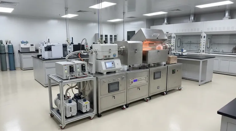
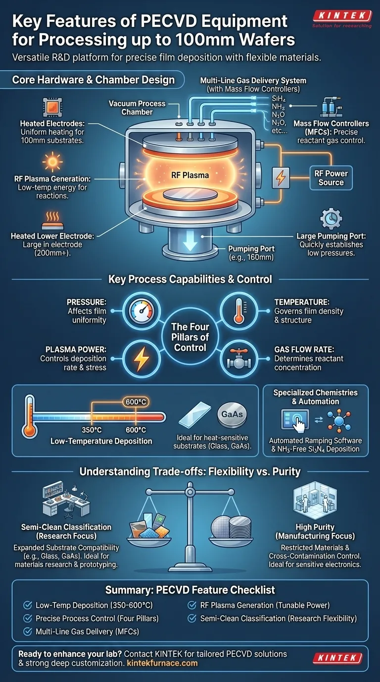
In essence, a PECVD system for 100mm wafers is a highly versatile deposition tool defined by its process flexibility and precise control over film properties. Key features include a vacuum chamber with heated electrodes, a multi-line gas delivery system with mass flow controllers, and radio frequency (RF) plasma generation, enabling the growth of quality films at temperatures far lower than conventional methods.
While specific models vary, PECVD equipment in this class is fundamentally a versatile research and development platform. Its primary value lies in its ability to deposit films on a wide variety of materials, a flexibility that is often prioritized over the extreme purity required for leading-edge semiconductor manufacturing.
Core Hardware and Chamber Design
The physical construction of a PECVD system is engineered for precise, repeatable control over the deposition environment.
The Process Chamber and Electrodes
A typical system is built around a vacuum process chamber. It features a heated upper electrode and a lower electrode, which holds the wafer and is often over 200mm in diameter to ensure uniform heating for a 100mm substrate. A large pumping port, such as a 160mm port, is critical for quickly establishing and maintaining the low pressures required for the process.
Gas Delivery System
Precise control of reactant gases is non-negotiable. These systems feature a sophisticated gas pod, often with a dozen or more gas lines. Each line is governed by a mass flow controller (MFC), which ensures the exact amount of each precursor gas enters the chamber, enabling repeatable and tunable film chemistry.
Plasma Generation and Control
The system uses a radio frequency (RF) power source to ignite the precursor gases into a plasma. This plasma provides the energy for the chemical reactions, which is why the process can run at low temperatures. The ability to control RF power is one of the primary levers for adjusting film properties like density and stress.
Key Process Capabilities and Control
The hardware features enable a wide range of process capabilities. Mastering the tool means understanding how to manipulate its core parameters.
The Four Pillars of PECVD Control
Film quality is determined by the interplay of four critical parameters:
- Pressure: Affects the mean free path of reactant species and influences film uniformity.
- Temperature: Governs the surface mobility of atoms, impacting film density and structure.
- Gas Flow Rate: Determines the concentration of reactants available for the deposition reaction.
- Plasma Power: Controls the energy of the reaction, affecting deposition rate and film stress.
Low-Temperature Deposition
The defining advantage of PECVD is its ability to deposit high-quality films at low temperatures, typically between 350°C and 600°C. This makes it possible to coat substrates that cannot withstand the high temperatures of conventional chemical vapor deposition (CVD), such as glass or certain compound semiconductors.
Specialized Film Chemistries
The hardware is often designed to facilitate specific, advanced chemistries. For example, some systems are built to enable ammonia-free (NH3-free) silicon nitride (Si3N4) deposition. This process is specifically designed to decrease the hydrogen (H2) content in the final film, improving its electrical and mechanical properties.
User Interface and Automation
Modern systems integrate these controls into a single interface, often a touch screen. They typically include parameter ramping software, which allows the user to program gradual changes in temperature, pressure, or gas flow during a run. This automation is crucial for process consistency and depositing complex film stacks.
Understanding the Trade-offs: Flexibility vs. Purity
The classification of a tool reveals its intended application and inherent limitations.
The "Semi-Clean" Classification
PECVD tools for 100mm wafers are often designated as "semi-clean." This signifies a more relaxed policy regarding the types of materials and substrates allowed in the chamber compared to tools used for pristine silicon manufacturing.
Expanded Substrate Compatibility
This semi-clean status is a major advantage for research environments. It allows the tool to process a diverse range of substrates beyond standard silicon, including glass wafers, glass slides, and Gallium Arsenide (GaAs), without violating tool protocols.
When to Use a More Restrictive Tool
In contrast, tools designed for larger wafers (e.g., 150mm and up) are often much more restrictive. These systems are typically reserved for processes where cross-contamination is a critical failure point, such as fabricating sensitive electronic devices. The flexibility of the 100mm tool comes at the cost of potential trace contamination.
Making the Right Choice for Your Goal
Selecting the appropriate tool depends entirely on your end goal.
- If your primary focus is materials research or prototyping: The substrate flexibility and relaxed material policy of a 100mm semi-clean PECVD system make it an ideal choice.
- If your primary focus is depositing high-purity films for sensitive electronics: A more restrictive, "clean" tool dedicated to a limited set of materials is necessary to avoid performance-killing cross-contamination.
- If your primary focus is process development: The precise, software-driven control over gas flow, power, and temperature makes this class of tool an excellent platform for optimizing film properties.
Ultimately, understanding these features empowers you to select not just a machine, but the right capability for your specific material science or fabrication objective.
Summary Table:
| Feature | Description |
|---|---|
| Low-Temperature Deposition | Operates at 350°C to 600°C, ideal for heat-sensitive substrates like glass and GaAs. |
| Precise Process Control | Manages pressure, temperature, gas flow, and plasma power for tunable film properties. |
| Multi-Line Gas Delivery | Uses mass flow controllers for accurate reactant gas handling and repeatable chemistry. |
| RF Plasma Generation | Enables energy-efficient film growth with adjustable power for density and stress control. |
| Semi-Clean Classification | Allows processing of diverse materials, supporting research flexibility over high purity. |
Ready to enhance your lab's capabilities with tailored PECVD solutions? At KINTEK, we leverage exceptional R&D and in-house manufacturing to provide advanced high-temperature furnace systems, including CVD/PECVD Systems. Our strong deep customization capability ensures we precisely meet your unique experimental requirements, whether for materials research, prototyping, or process development. Contact us today to discuss how our PECVD equipment can optimize your film deposition processes and drive innovation in your projects!
Visual Guide
Related Products
- Slide PECVD Tube Furnace with Liquid Gasifier PECVD Machine
- RF PECVD System Radio Frequency Plasma Enhanced Chemical Vapor Deposition
- Inclined Rotary Plasma Enhanced Chemical Deposition PECVD Tube Furnace Machine
- Inclined Rotary Plasma Enhanced Chemical Deposition PECVD Tube Furnace Machine
- Multi Heating Zones CVD Tube Furnace Machine for Chemical Vapor Deposition Equipment
People Also Ask
- What are the main advantages of PECVD tube furnaces compared to CVD tube furnaces? Lower Temp, Faster Deposition, and More
- What plasma source is used in PE-CVD tube furnaces? Unlock Low-Temperature, High-Quality Deposition
- What is plasma in the context of PECVD? Unlock Low-Temperature Thin Film Deposition
- How does PECVD equipment contribute to TOPCon bottom cells? Mastering Hydrogenation for Maximum Solar Efficiency
- What are the typical conditions for plasma-enhanced CVD processes? Achieve Low-Temperature Thin Film Deposition


