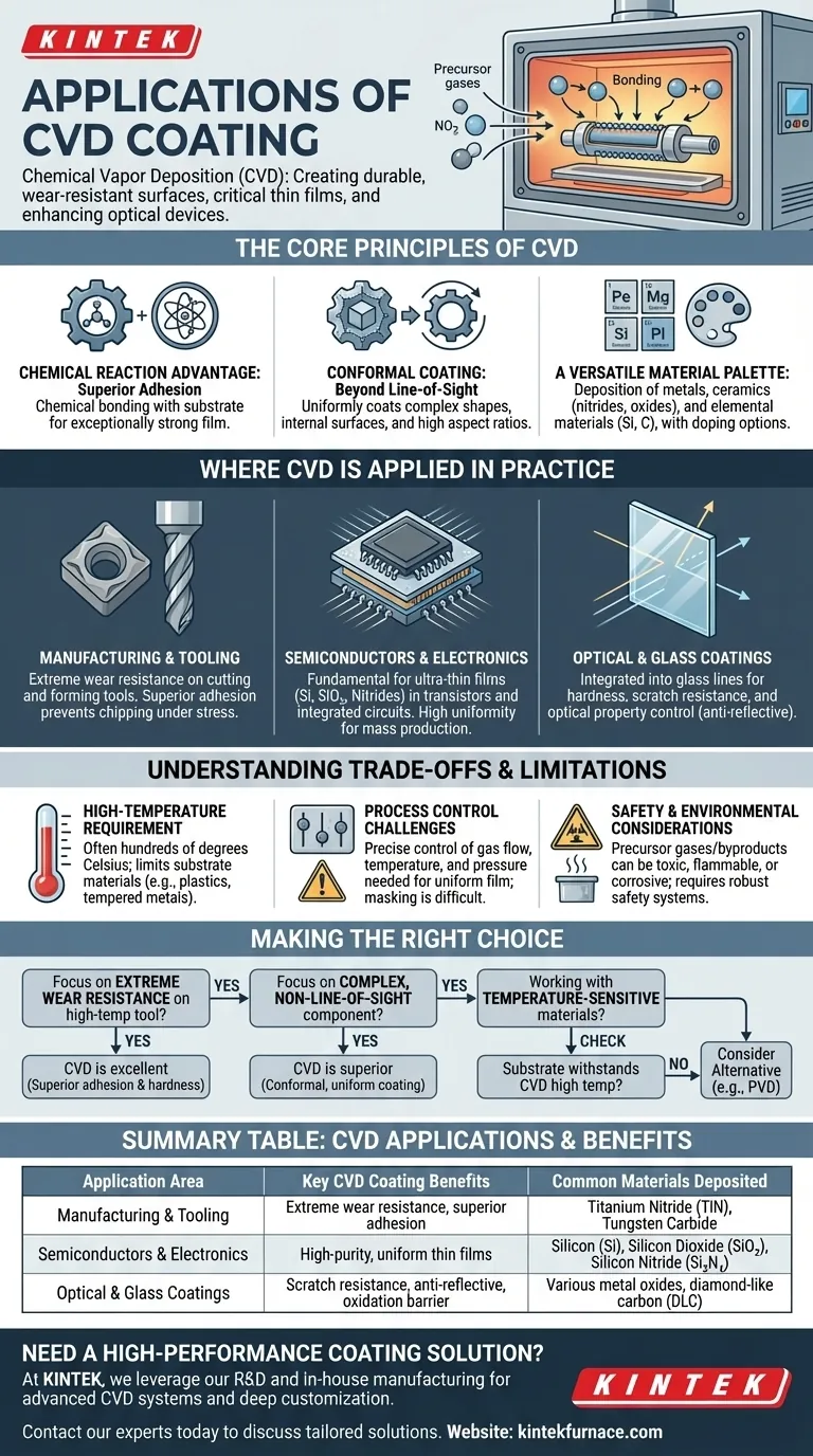
At its core, Chemical Vapor Deposition (CVD) is a highly versatile coating process used across a diverse range of industries. Its primary applications are creating extremely durable, wear-resistant surfaces for manufacturing tools, depositing critical thin films in the semiconductor industry, and enhancing the properties of optical devices and glass.
CVD is the preferred method when a highly adherent and uniform coating is required on a component, especially one with a complex shape. Its defining characteristic is a chemical reaction that bonds the coating to the surface, creating superior durability, but this requires high temperatures that limit the types of materials that can be coated.
The Core Principles of CVD
To understand its applications, you must first understand why CVD is chosen over other methods. Its unique gas-phase chemical reaction process provides distinct advantages.
The Chemical Reaction Advantage: Superior Adhesion
CVD is not merely layering a material onto a surface. The process involves introducing precursor gases into a high-temperature chamber, which then react and chemically bond with the substrate.
This creates an exceptionally strong, adherent film that becomes part of the substrate itself. This bond is often superior to the adhesion achieved with physical deposition methods.
Conformal Coating: Beyond Line-of-Sight
Because the coating is formed from a gas, it can flow into and around intricate features. This makes CVD ideal for uniformly coating complex shapes, internal surfaces, and components with high aspect ratios.
Unlike line-of-sight processes like PVD, CVD ensures that all surfaces are coated evenly, a critical requirement for many advanced components.
A Versatile Material Palette
CVD can be used to deposit a wide variety of materials. This includes metals, ceramics like nitrides and oxides, and elemental materials like silicon and carbon.
Furthermore, these materials can be "doped" during the process to functionalize the coating for specific performance goals, such as altering electrical conductivity in semiconductors.
Where CVD is Applied in Practice
The unique characteristics of the CVD process make it the ideal solution for several key industrial challenges.
Manufacturing and Tooling
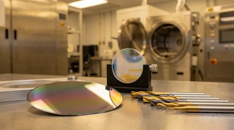
The most common application for CVD is creating wear-resistant coatings on metal-forming and cutting tools. Carbide milling inserts, turning tools, and other wear components benefit immensely from a hard coating like titanium nitride.
The superior adhesion from the CVD process ensures the coating does not chip or flake away under the extreme stress and heat of machining operations.
Semiconductors and Electronics
CVD is fundamental to modern electronics manufacturing. It is used to deposit the ultra-thin films of silicon, silicon dioxide, and various nitrides that form the building blocks of transistors and integrated circuits.
The process offers high deposition rates for mass production and the ability to create highly uniform layers, which is essential for the performance and reliability of microelectronic devices.
Optical and Glass Coatings
In the glass industry, CVD is often integrated directly into the float-glass manufacturing line. Gases are used to deposit thin, durable layers that improve the glass's properties.
These coatings can increase hardness, enhance scratch resistance, and change the optical properties to control reflection or transmission, all while preventing oxidation.
Understanding the Trade-offs and Limitations
While powerful, CVD is not a universal solution. Its process characteristics create specific limitations that must be considered.
The High-Temperature Requirement
CVD's primary drawback is its reliance on elevated temperatures (often several hundred degrees Celsius) to drive the chemical reaction.
This high heat limits the types of substrate materials that can be coated. Many plastics, tempered metals, or other temperature-sensitive materials would be damaged or warped by the process.
Process Control Challenges
Achieving a perfectly uniform film thickness requires precise control over gas flow, temperature, and pressure. Poor control can lead to variations or particle contamination within the coating.
Additionally, masking specific areas of a component to prevent them from being coated is significantly more difficult in CVD than in line-of-sight processes.
Safety and Environmental Considerations
The precursor gases and chemical byproducts generated during the CVD process are often toxic, flammable, or corrosive.
This necessitates sophisticated and expensive equipment for handling, as well as robust safety and environmental systems like cold traps or scrubbers to neutralize waste products.
Making the Right Choice for Your Application
Selecting the correct coating technology depends entirely on your material, component geometry, and performance goals.
- If your primary focus is extreme wear resistance on a high-temperature tool: CVD is an excellent choice due to its superior adhesion and ability to deposit exceptionally hard ceramic coatings.
- If your primary focus is coating a complex, non-line-of-sight component: CVD's ability to create a conformal, uniform coating on intricate geometries makes it a superior option.
- If you are working with temperature-sensitive materials like polymers or certain alloys: You must verify that the substrate can withstand CVD's high process temperatures or consider an alternative like Physical Vapor Deposition (PVD).
By understanding its unique chemical bonding process and inherent limitations, you can leverage CVD to create exceptionally durable and functional surfaces for the most demanding applications.
Summary Table:
| Application Area | Key CVD Coating Benefits | Common Materials Deposited |
|---|---|---|
| Manufacturing & Tooling | Extreme wear resistance, superior adhesion for cutting tools | Titanium Nitride (TiN), Tungsten Carbide |
| Semiconductors & Electronics | High-purity, uniform thin films for microelectronics | Silicon (Si), Silicon Dioxide (SiO₂), Silicon Nitride (Si₃N₄) |
| Optical & Glass Coatings | Scratch resistance, anti-reflective properties, oxidation barrier | Various metal oxides, diamond-like carbon (DLC) |
Need a high-performance coating solution for a demanding application?
At KINTEK, we leverage our exceptional R&D and in-house manufacturing to provide advanced high-temperature furnace solutions, including state-of-the-art CVD systems. Our product line is complemented by strong deep customization capabilities to precisely meet your unique experimental and production requirements.
Whether you are developing next-generation semiconductors, creating wear-resistant tooling, or enhancing optical components, our expertise can help you achieve superior results. Contact our experts today to discuss how we can tailor a solution for you.
Visual Guide
Related Products
- HFCVD Machine System Equipment for Drawing Die Nano Diamond Coating
- RF PECVD System Radio Frequency Plasma Enhanced Chemical Vapor Deposition
- Custom Made Versatile CVD Tube Furnace Chemical Vapor Deposition CVD Equipment Machine
- Multi Heating Zones CVD Tube Furnace Machine for Chemical Vapor Deposition Equipment
- Slide PECVD Tube Furnace with Liquid Gasifier PECVD Machine
People Also Ask
- What is the significance of the vacuum pressure control system in the CVD coating process for powders?
- What is the advantage of using a CVD system for coating turbine blades? Master Complex Geometries with Ease
- What materials are commonly used in CVD coating systems? Explore Key Materials for Superior Coatings
- What core function does CVD equipment serve in h-BN anti-corrosion? Master Precision Synthesis for High-Performance Films
- What is Hot-filament Chemical Vapor Deposition (HFCVD)? Achieve High-Quality Thin Films with Precision Control


