Chemical Vapor Deposition (CVD) is significantly superior to Liquid Phase Exfoliation (LPE) for preparing Bi2Se3 topological insulator films due to its ability to deliver structural precision. While LPE often results in irregular nanosheets with unpredictable properties, a CVD system provides a controlled environment that ensures highly uniform geometric shapes, superior crystal quality, and exact control over the number of growth layers.
Core Takeaway Liquid Phase Exfoliation (LPE) typically suffers from non-uniform morphology and uncontrollable absorption parameters, making it unsuitable for high-precision applications. In contrast, CVD offers the rigorous control necessary to produce high-quality, uniform crystals with specific layer counts, providing a reliable physical foundation for studying thickness-dependent properties.
Achieving Structural Precision
Control Over Growth Layers
The most critical advantage of a CVD system is the ability to precisely dictate the number of growth layers in the Bi2Se3 film. This capability is essential for researchers needing to investigate thickness-dependent properties, as the physical behavior of topological insulators changes significantly based on layer count.
Uniform Geometric Shapes
CVD systems produce films with highly uniform geometric shapes. This contrasts sharply with LPE, which frequently yields nanosheets with random, non-uniform morphologies that can compromise device performance.
Material Quality and Performance
Superior Crystal Quality
The controlled reaction environment of a CVD system facilitates the growth of films with superior crystallinity. By managing the transport of precursor vapors, CVD ensures the material achieves single-crystal characteristics and a flat surface morphology, acting as a high-quality platform for micro-nano device fabrication.
Predictable Optical Parameters
For applications involving optics, consistency is paramount. LPE often results in uncontrollable saturable absorption parameters due to its irregular output. CVD eliminates this variability, ensuring that the optical properties of the Bi2Se3 film remain stable and predictable.
Understanding the Trade-offs
The Cost of Variability
When choosing between these methods, the primary trade-off lies in the tolerance for irregularity. LPE lacks the "physical foundation" required for precision studies because its output varies too widely. If your application requires exact physical baselines—such as specific saturable absorption rates or layer counts—the randomness of LPE represents a technical debt that cannot be engineered away; CVD is the only viable path to mitigate this risk.
Making the Right Choice for Your Goal
To ensure your fabrication method aligns with your technical requirements, consider the following:
- If your primary focus is studying thickness-dependent properties: You must use CVD to ensure precise control over the number of layers and crystal uniformity.
- If your primary focus is consistent device performance: You should utilize CVD to avoid the uncontrollable saturable absorption parameters inherent to LPE.
- If your primary focus is high-quality micro-nano fabrication: Rely on CVD to provide a flat, single-crystal foundation that LPE cannot replicate.
Select the method that guarantees the structural integrity required for your specific application.
Summary Table:
| Feature | Liquid Phase Exfoliation (LPE) | Chemical Vapor Deposition (CVD) |
|---|---|---|
| Layer Control | Random / Unpredictable | Precise Atomic Layer Control |
| Morphology | Irregular Nanosheets | Highly Uniform Geometric Shapes |
| Crystal Quality | Variable / Lower | Superior Single-Crystal Quality |
| Repeatability | Low (Inconsistent Parameters) | High (Predictable Performance) |
| Best For | Bulk Material Processing | High-Precision Micro-Nano Devices |
Elevate Your Thin-Film Research with KINTEK
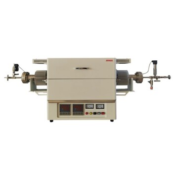
Don't let the unpredictability of LPE hinder your breakthroughs. KINTEK provides industry-leading Chemical Vapor Deposition (CVD) systems tailored for researchers who demand structural precision and repeatable results.
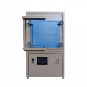
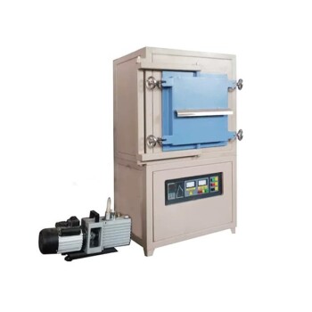
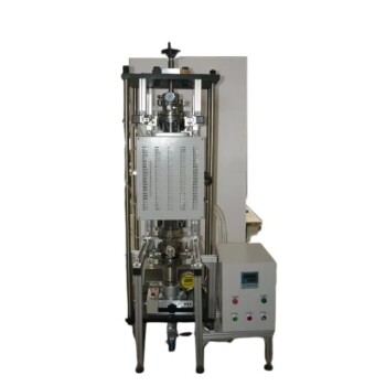
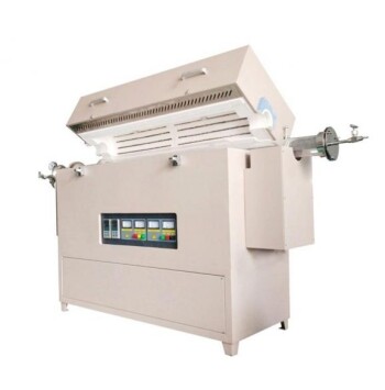
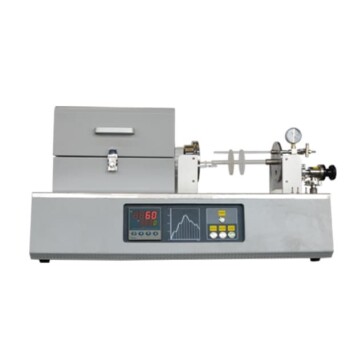
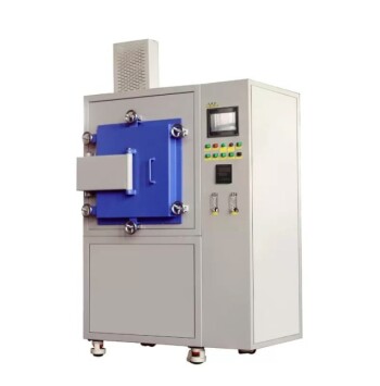
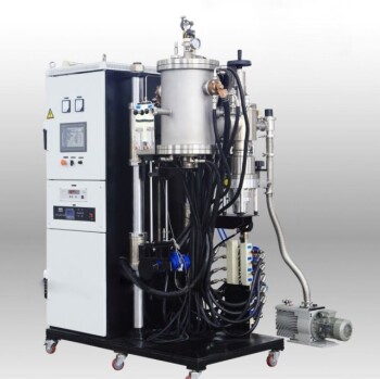
Backed by expert R&D and manufacturing, KINTEK offers CVD, Muffle, Tube, Rotary, and Vacuum systems, all fully customizable to meet the unique needs of your topological insulator studies. Ensure your materials have the high-quality physical foundation they deserve.
Contact KINTEK Experts Today for a Custom Quote
References
- Yang Gao, Fei Chen. Study on Saturable Absorption Characteristics of Bi2Se3 Topological Insulators with Film Thickness Dependence and Its Laser Application. DOI: 10.3390/coatings14060679
This article is also based on technical information from Kintek Furnace Knowledge Base .
Related Products
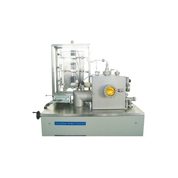
- Inclined Rotary Plasma Enhanced Chemical Deposition PECVD Tube Furnace Machine
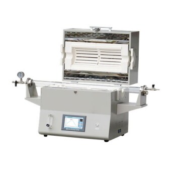
- Multi Heating Zones CVD Tube Furnace Machine for Chemical Vapor Deposition Equipment
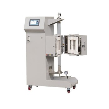
- Vertical Laboratory Quartz Tube Furnace Tubular Furnace
- 1400℃ High Temperature Laboratory Tube Furnace with Alumina Tube
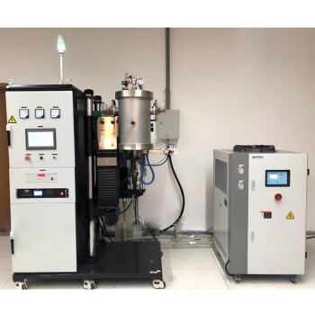
- Vacuum Heat Treat Sintering Furnace Molybdenum Wire Vacuum Sintering Furnace
People Also Ask
- What methods are used to analyze and characterize graphene samples? Unlock Key Techniques for Accurate Material Analysis
- How does a CVD system ensure the quality of carbon layers? Achieving Nanometer Precision with KINTEK
- What are the future trends in CVD technology? AI, Sustainability, and Advanced Materials
- What are the technical advantages of using a CVD system? Optimize Carbon Nanotube Growth for Thermal Conductivity
- Why Use PECVD for Monolithic Integrated Chip Isolation Layers? Protect Your Thermal Budget with High-Quality SiO2
