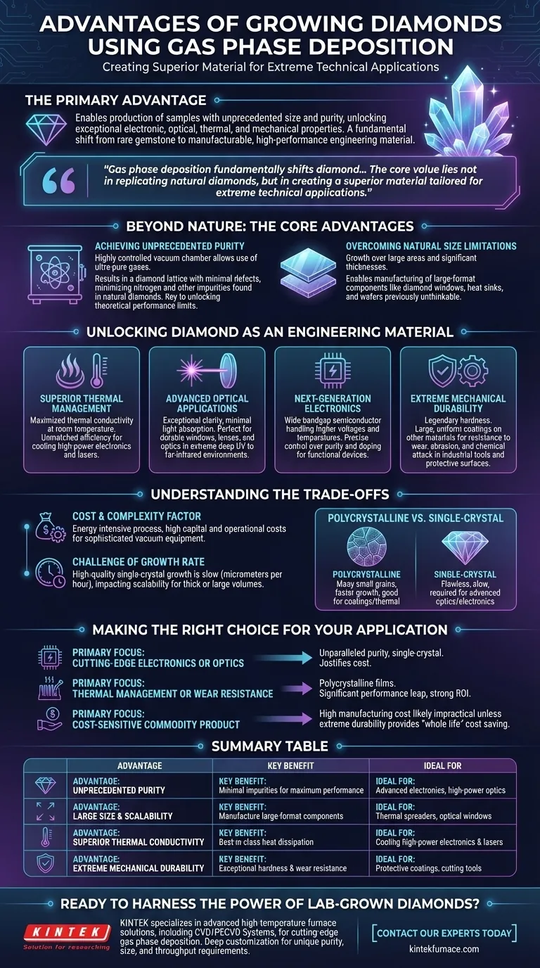
The primary advantage of growing diamonds using gas phase deposition is the ability to create samples with a combination of size and purity that is virtually impossible to achieve through natural geological processes or other synthesis methods. This technique unlocks the material's full potential, enabling the production of high-performance components with exceptional electronic, optical, thermal, and mechanical properties.
Gas phase deposition fundamentally shifts diamond from a rare gemstone to a manufacturable, high-performance engineering material. The core value lies not in replicating natural diamonds, but in creating a superior material tailored for extreme technical applications.
Beyond Nature: The Core Advantages
The method's significance comes from overcoming two fundamental limitations of both natural and other synthetic diamonds: impurities and size constraints.
Achieving Unprecedented Purity
Natural diamonds form in an uncontrolled geological environment, inevitably incorporating impurities like nitrogen, which affect their color and properties.
Gas phase deposition, however, occurs in a highly controlled vacuum chamber. This allows for the use of exceptionally pure source gases, resulting in a diamond lattice with minimal defects or foreign atoms. This ultra-high purity is the key to unlocking its theoretical performance limits.
Overcoming Natural Size Limitations
Large, flawless natural diamonds are exceptionally rare and astronomically expensive. This has historically prevented diamond from being considered a viable material for large-format components.
Gas phase deposition allows for growth over large areas and to significant thicknesses. This makes it possible to manufacture diamond windows, heat sinks, and wafers on a scale that was previously unthinkable.
Unlocking Diamond as an Engineering Material
The combination of high purity and large size directly translates into superior material properties, opening the door to a new class of technological applications.
Superior Thermal Management
Diamond is the most thermally conductive material at room temperature. The purity achieved through gas phase deposition ensures this conductivity is maximized, allowing heat to dissipate with unmatched efficiency. This makes it a critical material for cooling high-power electronics and lasers.
Advanced Optical Applications
Impurities in a diamond absorb and scatter light, which can lead to damage when used with high-power lasers. The clarity of gas-phase-grown diamonds makes them perfect for durable windows, lenses, and other optical components in extreme environments, from deep UV to far-infrared.
Next-Generation Electronics
Diamond is a wide-bandgap semiconductor, meaning it can handle much higher voltages and temperatures than silicon. Creating functional diamond-based electronics requires precise control over purity and the ability to intentionally add specific impurities (doping). Gas phase deposition provides this essential level of control.
Extreme Mechanical Durability
The hardness of diamond is legendary. Being able to deposit large, uniform, and pure diamond coatings onto other materials dramatically increases their resistance to wear, abrasion, and chemical attack. This is invaluable for industrial cutting tools, durable optics, and protective surfaces.
Understanding the Trade-offs
While the advantages are significant, this technology is not a universal solution. It involves key trade-offs that are critical to understand for any practical application.
The Cost and Complexity Factor
Gas phase deposition is an energy-intensive process that requires sophisticated, high-cost vacuum equipment. The initial capital investment and operational costs are substantial compared to traditional materials.
The Challenge of Growth Rate
Growing high-quality, single-crystal diamond is an exceptionally slow process, often measured in micrometers per hour. This low throughput directly impacts the cost and scalability for producing very thick or large-volume diamond components.
Polycrystalline vs. Single-Crystal
For many applications, like coatings and heat spreaders, a polycrystalline film (composed of many small crystal grains) is sufficient and faster to grow. However, for advanced optical or electronic applications, a flawless single-crystal structure is required, which is far more challenging and time-consuming to produce.
Making the Right Choice for Your Application
Selecting the right material requires aligning the benefits of gas-phase-grown diamond with your specific technical and budgetary goals.
- If your primary focus is cutting-edge electronics or optics: The unparalleled purity and controlled growth of single-crystal diamond are essential and justify the cost.
- If your primary focus is thermal management or wear resistance: Polycrystalline diamond films offer a significant performance leap over conventional materials and may provide a strong return on investment.
- If your primary focus is a cost-sensitive commodity product: The high manufacturing cost will likely make gas-phase-grown diamond impractical unless its extreme durability creates a "whole life" cost saving.
Ultimately, gas phase deposition empowers engineers and scientists to use diamond not for what it has been, but for what it can be.
Summary Table:
| Advantage | Key Benefit | Ideal For |
|---|---|---|
| Unprecedented Purity | Minimal impurities for maximum performance | Advanced electronics, high-power optics |
| Large Size & Scalability | Manufacture large-format components | Thermal spreaders, optical windows |
| Superior Thermal Conductivity | Best-in-class heat dissipation | Cooling high-power electronics & lasers |
| Extreme Mechanical Durability | Exceptional hardness & wear resistance | Protective coatings, cutting tools |
Ready to harness the power of lab-grown diamonds for your most demanding applications?
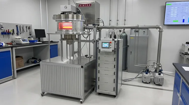
KINTEK specializes in providing the advanced high-temperature furnace solutions, including our CVD/PECVD Systems, that are essential for cutting-edge gas phase deposition processes. Our deep customization capabilities ensure your equipment is precisely tailored to meet the unique purity, size, and throughput requirements of your diamond growth R&D or production.
Contact our experts today to discuss how we can help you build a superior diamond synthesis solution.
Visual Guide
Related Products
- 915MHz MPCVD Diamond Machine Microwave Plasma Chemical Vapor Deposition System Reactor
- HFCVD Machine System Equipment for Drawing Die Nano Diamond Coating
- MPCVD Machine System Reactor Bell-jar Resonator for Lab and Diamond Growth
- Cylindrical Resonator MPCVD Machine System for Lab Diamond Growth
- Slide PECVD Tube Furnace with Liquid Gasifier PECVD Machine
People Also Ask
- In which industries is the microwave plasma chemical vapor deposition system commonly used? Unlock High-Purity Material Synthesis
- What is the basic principle of operation for the microwave plasma chemical vapor deposition system? Unlock High-Purity Material Growth
- What is the purpose of a microwave plasma chemical vapor deposition system? Grow High-Purity Diamonds and Advanced Materials
- What are the essential components of an MPCVD reactor for diamond film deposition? Unlock High-Quality Diamond Growth
- What factors influence the quality of diamond deposition in the MPCVD method? Master the Critical Parameters for High-Quality Diamond Growth


