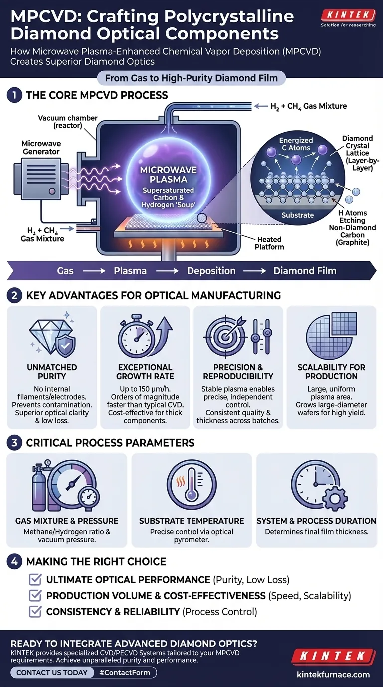
In short, Microwave Plasma-Enhanced Chemical Vapor Deposition (MPCVD) manufactures diamond optical components by using microwave energy to create a highly controlled plasma. This plasma contains energized carbon and hydrogen atoms, which are then deposited layer-by-layer onto a substrate, growing a pure, high-quality polycrystalline diamond film. This film can be shaped into superior optical components like windows, lenses, and prisms.
The critical insight is that MPCVD has become the dominant industrial method not just because it can grow diamond, but because it solves the core manufacturing challenges of purity, speed, and control. It creates optical-grade diamond cleanly and repeatably, a feat that older methods struggle to achieve at scale.
The Core MPCVD Process: From Gas to Diamond
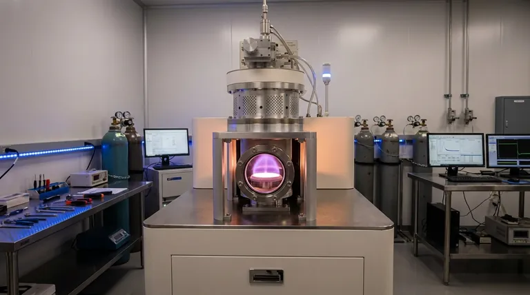
To understand why MPCVD is so effective, we must look at how it transforms simple gas into one of the world's hardest and most optically transparent materials. The process occurs within a highly controlled vacuum chamber, which is the heart of the MPCVD reactor.
Generating the Plasma: The Role of Microwaves
The process begins by introducing a precise mixture of gases, typically hydrogen and a carbon-containing gas like methane, into the chamber. A generator then floods the chamber with microwaves.
This microwave energy excites the gas, stripping electrons from atoms and creating a plasma—a glowing ball of ionized gas. The oscillating electromagnetic field causes violent collisions, producing a very high-density, stable plasma that is ideal for diamond growth.
The Deposition Environment: Supersaturated Carbon
This high-density plasma is a "soup" of supersaturated carbon and hydrogen atomic groups. It creates the perfect chemical environment for carbon atoms to arrange themselves into the strong tetrahedral bonds of a diamond crystal lattice on the substrate surface.
The hydrogen plays a crucial role by selectively etching away any non-diamond carbon (like graphite), ensuring the growing film is of exceptionally high purity.
Building the Diamond Film: Layer-by-Layer Growth
The prepared substrate, heated to a precise temperature, acts as the foundation. The energized carbon atoms from the plasma deposit onto its surface, forming a polycrystalline diamond film.
This process continues, building the diamond layer by atomic layer, until the desired thickness is achieved. The final material possesses a broad transparency range, high refractive index, and extremely low optical loss.
Key Advantages of MPCVD for Optical Manufacturing
MPCVD is not the only way to synthesize diamond, but its specific characteristics make it uniquely suited for producing high-performance optics.
Unmatched Purity: Avoiding Contamination
Unlike older methods such as Hot Filament CVD (HFCVD), the MPCVD plasma is generated without electrodes or filaments inside the chamber. This eliminates a major source of contamination, resulting in a chemically purer diamond film with superior optical properties.
Exceptional Growth Rate and Efficiency
Modern MPCVD systems can achieve growth rates up to 150 μm/h. This is orders of magnitude faster than typical CVD processes and is critical for making the production of thick optical components economically viable.
Precision and Reproducibility
The stability of the microwave-generated plasma allows for precise, independent control over key parameters. This stability ensures that every production run yields diamond of a consistent quality and thickness, a non-negotiable requirement for high-end optics.
Scalability for Industrial Production
MPCVD reactors can create a large, uniform plasma area. This enables the growth of large-diameter diamond wafers, which can then be cut into multiple smaller optical components, making the process highly scalable for industrial demand.
Understanding the Critical Process Parameters
The success of the MPCVD process hinges on meticulous control over several interconnected variables. Mismanaging these parameters can compromise the quality of the final diamond component.
The Gas Mixture and Pressure
The ratio of methane to hydrogen in the gas mixture directly influences the quality and growth rate of the diamond. The pressure within the vacuum chamber must also be carefully regulated to maintain the stability and density of the plasma.
Substrate Temperature Control
Temperature is one of the most critical factors. If the substrate is too cold, growth slows down. If it is too hot, the formation of undesirable graphite (soot) can occur instead of diamond. An optical pyrometer is used to monitor and maintain the temperature with extreme precision.
System and Process Duration
The entire system—from the microwave generator and gas flow controllers to the vacuum pumps and cooling chillers—must work in perfect concert. The duration of the deposition process is simply determined by the desired thickness of the final diamond film.
Making the Right Choice for Your Application
Understanding the strengths of MPCVD allows you to specify materials with confidence, knowing the underlying manufacturing process is robust and reliable.
- If your primary focus is ultimate optical performance and purity: MPCVD is the superior choice for applications where even minute impurities can degrade performance, such as in high-power lasers or sensitive sensors.
- If your primary focus is production volume and cost-effectiveness: MPCVD's high growth rates and scalability make it the only practical choice for manufacturing diamond optics in industrial quantities.
- If your primary focus is consistency and reliability across batches: The exceptional process control of MPCVD ensures that optical components produced today will match the specifications of those produced months from now.
Ultimately, mastering the MPCVD process allows us to harness the remarkable properties of diamond for demanding optical applications with unparalleled precision.
Summary Table:
| Key MPCVD Advantage | Benefit for Optical Manufacturing |
|---|---|
| Unmatched Purity | No internal filaments/electrodes prevents contamination, ensuring superior optical clarity and low loss. |
| High Growth Rate (up to 150 μm/h) | Enables cost-effective production of thick optical components at an industrial scale. |
| Precise Process Control | Guarantees consistent quality, thickness, and optical properties across all production batches. |
| Scalable Plasma Area | Allows for the growth of large-diameter diamond wafers, increasing yield and efficiency. |
Ready to Integrate Advanced Diamond Optics into Your Systems?
Leveraging exceptional R&D and in-house manufacturing, KINTEK provides diverse laboratories with advanced high-temperature furnace solutions, including specialized CVD/PECVD Systems. Our strong deep customization capability allows us to precisely tailor our equipment to meet your unique MPCVD process requirements for growing high-quality polycrystalline diamond.
Contact us today to discuss how our solutions can help you achieve unparalleled purity and performance in your optical components.
Visual Guide
Related Products
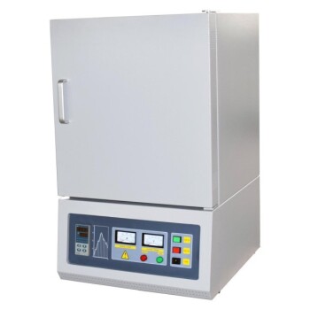
- Multi Heating Zones CVD Tube Furnace Machine for Chemical Vapor Deposition Equipment
- 915MHz MPCVD Diamond Machine Microwave Plasma Chemical Vapor Deposition System Reactor
- Multi Zone Laboratory Quartz Tube Furnace Tubular Furnace
- Inclined Rotary Plasma Enhanced Chemical Deposition PECVD Tube Furnace Machine
- Inclined Rotary Plasma Enhanced Chemical Deposition PECVD Tube Furnace Machine
People Also Ask
- What role do multi zone tube furnaces play in new energy research? Unlock Precise Thermal Control for Innovation
- What are the advantages of multi-zone tube furnaces? Achieve Superior Thermal Control for Advanced Materials Processing
- Why are multi zone tube furnaces particularly useful for nanomaterial research? Unlock Precise Thermal Control for Advanced Synthesis
- What role does a Tube Furnace play in the CVD growth of carbon nanotubes? Achieve High-Purity CNT Synthesis
- What is the function of a multi-zone tube furnace in CVD synthesis? Master 2D In2Se3 Nanosheet Precision