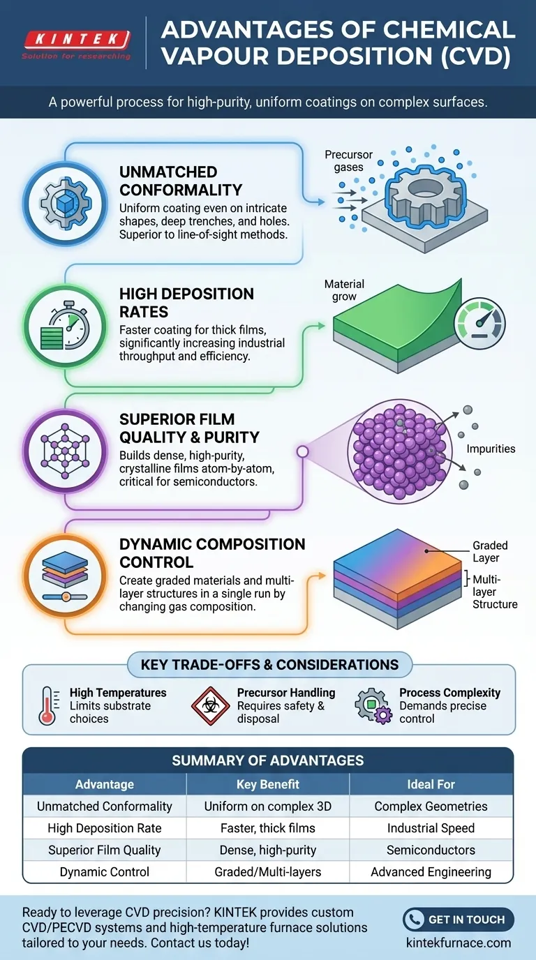
In essence, the primary advantages of Chemical Vapour Deposition (CVD) are its exceptional ability to apply uniform coatings over complex 3D surfaces, its high deposition speed, and its flexibility in creating high-purity films with tailored compositions. This process is a cornerstone of the semiconductor industry precisely because the chemical reaction at the heart of CVD allows for a level of control and quality that is difficult to achieve with other methods.
While many coating techniques exist, CVD's unique strength is its use of a chemical reaction. This allows it to "grow" a high-quality, solid film from gas precursors, enabling it to perfectly conform to intricate shapes and build complex material structures layer by layer.
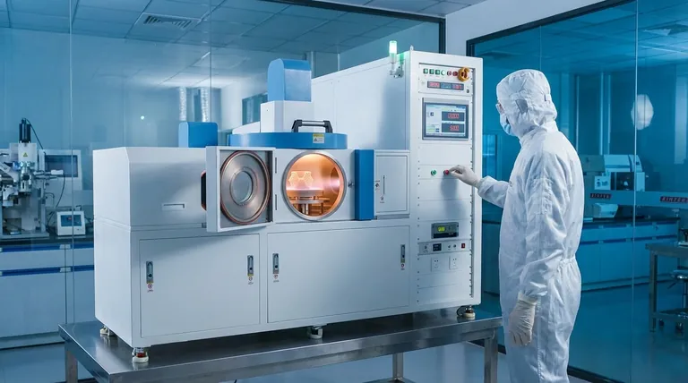
How Chemical Vapour Deposition Works
Chemical Vapour Deposition is a process where a substrate (the object to be coated) is placed in a reaction chamber and exposed to one or more volatile chemical precursors.
When these precursor gases interact on or near the heated substrate surface, they react or decompose, leaving behind a solid material in the form of a thin film. The other byproducts of the reaction are then vented out of the chamber.
Think of it not as spraying a surface, but as creating the conditions for a material to grow directly onto the substrate from a carefully controlled chemical atmosphere.
The Core Advantages of CVD Explained
The unique nature of this process gives rise to several significant advantages, making it the preferred choice for many high-performance applications.
Unmatched Conformality on Complex Surfaces
The precursor gases in a CVD process flow around the substrate, reaching every exposed area. The chemical reaction happens wherever the conditions (like temperature) are right.
This results in an exceptionally conformal coating. The film's thickness is highly uniform, even inside deep trenches, holes, and on complex three-dimensional geometries. This is a major advantage over line-of-sight methods like Physical Vapour Deposition (PVD), which can struggle to coat shadowed areas.
High Deposition Rates for Efficiency
CVD processes can often deposit material much faster than many competing techniques.
This high deposition rate makes CVD economically viable for producing relatively thick films, reducing manufacturing time and increasing throughput for industrial applications.
Superior Film Quality and Purity
Because CVD builds a film atom by atom through a chemical reaction, it can produce materials that are incredibly dense, pure, and have a highly ordered crystalline structure.
This control over film quality is critical in the semiconductor industry, where even minute impurities or structural defects in a thin film can render a microchip useless.
Dynamic Control Over Material Composition
During a single deposition run, the composition of the precursor gases can be changed.
This allows for the creation of functionally graded materials, where the composition changes throughout the film's thickness. You can also deposit distinct layers of different materials on top of each other without breaking the vacuum, creating complex multi-layer structures.
Understanding the Trade-offs
No process is perfect. To make an informed decision, it's crucial to understand the challenges associated with CVD.
High Temperature Requirements
Many CVD processes require high substrate temperatures, often several hundred degrees Celsius, to drive the necessary chemical reactions.
This can limit the types of substrate materials that can be coated, as some plastics or other temperature-sensitive materials may be damaged or melt.
Precursor and Byproduct Handling
The precursor chemicals used in CVD can be toxic, flammable, or corrosive.
Proper handling, storage, and disposal procedures are critical for safety and environmental compliance. Similarly, the gaseous byproducts of the reaction must be safely treated before being vented.
Process Complexity
Optimizing a CVD process involves a complex interplay of variables, including temperature, pressure, gas flow rates, and chamber chemistry.
Achieving a stable and repeatable process requires significant expertise and sophisticated control equipment. While it doesn't always require an ultra-high vacuum like some methods, it is still fundamentally a vacuum-based process that demands precise control.
Making the Right Choice for Your Application
Selecting the right deposition method depends entirely on your project's specific requirements.
- If your primary focus is coating a complex 3D part with a uniform film: CVD's excellent conformality makes it the superior choice.
- If your primary focus is producing high-purity, crystalline films for electronics: CVD offers the atomic-level control necessary for high-performance materials.
- If your primary focus is depositing a thick film quickly and efficiently: CVD's high deposition rates are a significant advantage.
- If you are coating a simple, flat surface and cost is the main driver: A simpler, line-of-sight technique like sputtering (a PVD method) might be more suitable.
Ultimately, the power of CVD lies in its ability to translate precise chemical control into high-performance, functional materials.
Summary Table:
| Advantage | Key Benefit | Ideal For |
|---|---|---|
| Unmatched Conformality | Uniform coating even on complex 3D surfaces, trenches, and holes | Complex geometries requiring consistent coverage |
| High Deposition Rate | Faster coating process, enabling thick films and high throughput | Industrial applications needing efficiency and speed |
| Superior Film Quality & Purity | Dense, high-purity, crystalline films with minimal defects | Semiconductor, electronics, and high-performance material applications |
| Dynamic Composition Control | Ability to create graded materials and multi-layer structures without breaking vacuum | Advanced material engineering and complex film architectures |
Ready to leverage the precision of CVD for your advanced coating needs?
At KINTEK, we combine exceptional R&D with in-house manufacturing to deliver advanced high-temperature furnace solutions tailored to your unique requirements. Our product line—including Tube Furnaces, Vacuum & Atmosphere Furnaces, and CVD/PECVD Systems—is designed to support high-purity, uniform deposition on complex surfaces. With our deep customization capabilities, we can help you achieve the precise chemical control needed for superior film quality and performance.
Contact us today to discuss how our CVD solutions can enhance your laboratory's capabilities → Get in Touch
Visual Guide
Related Products
- Custom Made Versatile CVD Tube Furnace Chemical Vapor Deposition CVD Equipment Machine
- RF PECVD System Radio Frequency Plasma Enhanced Chemical Vapor Deposition
- MPCVD Machine System Reactor Bell-jar Resonator for Lab and Diamond Growth
- Slide PECVD Tube Furnace with Liquid Gasifier PECVD Machine
- 915MHz MPCVD Diamond Machine Microwave Plasma Chemical Vapor Deposition System Reactor
People Also Ask
- Why are CVD tube furnace sintering systems indispensable for 2D material research and production? Unlock Atomic-Scale Precision
- What future trends are expected in the development of CVD tube furnaces? Discover Smarter, More Versatile Systems
- What is a CVD tube furnace and what is its primary function? Discover Precision Thin-Film Deposition
- What customization options are available for CVD tube furnaces? Tailor Your System for Superior Material Synthesis
- What are the key application fields of CVD tube furnaces? Unlock Precision in Thin-Film Synthesis


