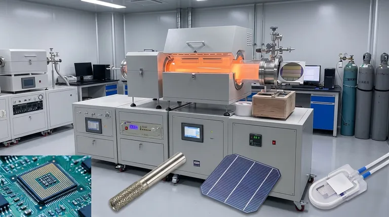
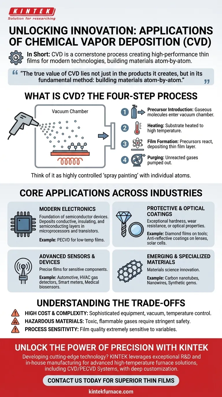
In short, Chemical Vapor Deposition (CVD) is a cornerstone manufacturing process used to create the high-performance thin films that power countless modern technologies. Its applications range from the microprocessors in smartphones and computers to durable coatings on cutting tools and the advanced sensors found in cars and smart homes.
The true value of CVD lies not just in the products it creates, but in its fundamental method: building materials atom-by-atom. This atomic-level control is what enables the creation of ultra-pure, exceptionally thin, and highly engineered films that are essential for high-performance electronics and advanced materials.
First, What Is Chemical Vapor Deposition?
At its core, Chemical Vapor Deposition is a process for depositing a solid material from a gaseous state onto a surface, known as a substrate. Think of it as a highly controlled and precise form of "spray painting" with individual atoms or molecules.
The Four-Step Process
The operation occurs inside a vacuum chamber and generally follows four critical steps:
- Precursor Introduction: Gaseous molecules, called precursors, are introduced into the chamber. These gases contain the atoms needed for the final film (e.g., silicon, carbon).
- Heating: The substrate is heated to a specific, high temperature. This energy is what drives the chemical reaction.
- Film Formation: The hot surface causes the precursor gases to react or decompose, depositing a solid, thin film layer onto the substrate, molecule by molecule.
- Purging: Once the desired thickness is achieved, the chamber is cooled, and any unreacted gases are pumped out.
This highly controlled environment ensures the resulting film is exceptionally pure and uniform.
Core Applications Across Industries
The ability to create such precise layers makes CVD indispensable across a vast range of fields. The applications are not just about coating a surface, but about building in specific electronic, optical, or protective properties.
The Foundation of Modern Electronics
This is the most significant application of CVD. Virtually every modern semiconductor device relies on it.
CVD is used to deposit the critical thin-film layers—conductive, insulating, and semiconducting—that form the transistors and wiring within a microchip. This includes a specialized variant, Plasma-Enhanced CVD (PECVD), which allows deposition at lower temperatures.
Protective and Optical Coatings
CVD is used to create surfaces with exceptional hardness, wear resistance, or specific optical properties.
For example, diamond films can be grown on cutting tools to dramatically increase their lifespan. In optics, CVD applies anti-reflective or protective coatings to lenses and solar cells (photovoltaics).
Advanced Sensors and Devices
The precision of CVD is ideal for manufacturing the sensitive components inside modern sensors.
These films are critical for automotive sensors (measuring pressure and acceleration), HVAC sensors (detecting gases), smart utility meters, and even medical biosensors that detect specific biological molecules.
Emerging and Specialized Materials
CVD is at the forefront of materials science innovation.
Specialized systems are used to grow advanced materials like carbon nanotubes and nanowires, which have revolutionary potential in electronics, medicine, and material processing. It is also used to create high-purity synthetic gems for industrial and electronic use.
Understanding the Trade-offs
While powerful, CVD is not a universal solution. Its precision comes with significant technical and financial considerations.
High Cost and Complexity
CVD systems are sophisticated machines requiring high vacuum, precise temperature control (from 600°C to over 2300°C), and automated gas handling. This represents a significant capital investment and requires specialized operational expertise.
Hazardous Materials
The precursor gases used in CVD are often toxic, flammable, or corrosive. This necessitates stringent safety protocols, handling infrastructure, and exhaust management, adding to the overall complexity and cost.
Process Sensitivity
The quality of the final film is extremely sensitive to variations in temperature, pressure, and gas flow. Achieving perfect uniformity, especially over large substrates, is a persistent engineering challenge that requires constant process optimization.
How to Apply This to Your Goal
Your choice to use or specify a CVD process depends entirely on the properties you need to engineer into a material's surface.
- If your primary focus is electronic performance: CVD is the non-negotiable, industry-standard process for building the fundamental layers of microchips and semiconductors.
- If your primary focus is surface durability or function: CVD provides a path to creating ultra-hard, wear-resistant, or optically-tuned surfaces that are integrated at an atomic level, not just painted on.
- If your primary focus is materials innovation: Advanced CVD systems are the essential tool for fabricating next-generation materials like carbon nanotubes and synthetic diamond films.
Ultimately, Chemical Vapor Deposition is the foundational process that translates atomic-level precision into real-world technological advancement.
Summary Table:
| Application Area | Key Examples |
|---|---|
| Electronics | Microprocessors, semiconductors, PECVD for low-temperature films |
| Protective & Optical Coatings | Diamond films on tools, anti-reflective coatings on lenses and solar cells |
| Sensors | Automotive sensors, HVAC gas detectors, medical biosensors |
| Advanced Materials | Carbon nanotubes, nanowires, synthetic gems |
Unlock the Power of Precision with KINTEK
Are you developing cutting-edge electronics, durable coatings, or innovative sensors? KINTEK leverages exceptional R&D and in-house manufacturing to provide advanced high-temperature furnace solutions tailored to your needs. Our product line—including Muffle, Tube, Rotary Furnaces, Vacuum & Atmosphere Furnaces, and CVD/PECVD Systems—is backed by strong deep customization capabilities to precisely meet your unique experimental requirements.
Contact us today to discuss how our CVD systems can enhance your research and production, delivering superior thin films and accelerating your technological advancements!
Visual Guide
Related Products
- Custom Made Versatile CVD Tube Furnace Chemical Vapor Deposition CVD Equipment Machine
- RF PECVD System Radio Frequency Plasma Enhanced Chemical Vapor Deposition
- MPCVD Machine System Reactor Bell-jar Resonator for Lab and Diamond Growth
- Slide PECVD Tube Furnace with Liquid Gasifier PECVD Machine
- 915MHz MPCVD Diamond Machine Microwave Plasma Chemical Vapor Deposition System Reactor
People Also Ask
- Which industries and research fields benefit from CVD tube furnace sintering systems for 2D materials? Unlock Next-Gen Tech Innovations
- What temperature range do standard CVD tube furnaces operate at? Unlock Precision for Your Material Deposition
- What are the key application fields of CVD tube furnaces? Unlock Precision in Thin-Film Synthesis
- What future trends are expected in the development of CVD tube furnaces? Discover Smarter, More Versatile Systems
- What is the working principle of a CVD tube furnace? Achieve Precise Thin Film Deposition for Your Lab


