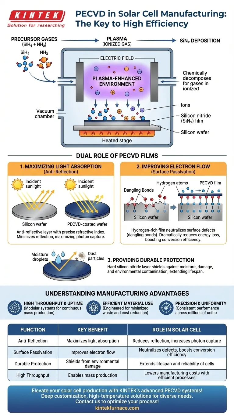
At its core, Plasma Enhanced Chemical Vapor Deposition (PECVD) is used in solar cell manufacturing to deposit exceptionally thin and uniform films onto silicon wafers. These films, primarily silicon nitride (SiNx), serve a dual purpose: they act as an anti-reflective coating to maximize sunlight absorption and as a passivation layer to improve the cell's electrical efficiency.
PECVD is not merely a coating step; it is a critical engineering process that directly enhances a solar cell's ability to both capture photons and efficiently convert them into electrical current, making it indispensable for modern, high-efficiency photovoltaic production.
The Dual Role of PECVD Films in Solar Efficiency
The films deposited by PECVD are not passive layers. They actively improve the performance of the solar cell in two distinct and crucial ways.
Function 1: Maximizing Light Absorption (Anti-Reflection)
A bare silicon wafer is naturally reflective, meaning it bounces a portion of sunlight away before it can be converted into electricity.
PECVD is used to apply a precise layer of silicon nitride. This film is engineered to have a specific refractive index that minimizes light reflection across the solar spectrum, ensuring more photons enter the active silicon material.
Function 2: Improving Electron Flow (Surface Passivation)
The surface of a silicon wafer has microscopic imperfections, often called "dangling bonds" or dislocations. These defects can trap the electrons that are freed by sunlight, causing them to lose their energy as heat instead of contributing to the electrical current.
The silicon nitride films deposited by PECVD are rich in hydrogen. This hydrogen "passivates" or neutralizes the surface defects, effectively healing them. This process dramatically reduces the loss of charge carriers, which directly increases the cell's overall conversion efficiency.
Function 3: Providing Durable Protection
In addition to its optical and electrical roles, the hard silicon nitride layer provides a durable coating that protects the sensitive silicon surface from moisture, handling damage, and environmental contamination over the life of the solar panel.
How the PECVD Process Achieves This
The precision of PECVD is what makes it so valuable. The process takes place in a highly controlled environment to build the film one molecular layer at a time.
The Plasma-Enhanced Environment
The entire process occurs within a vacuum chamber at very low pressure. A cyclical electric field is applied between two electrodes inside the chamber.
Using Precursor Gases
A carefully controlled mixture of precursor gases is introduced into the chamber. To create silicon nitride (SiNx), these gases are typically silane (SiH4) and ammonia (NH3), often mixed with inert carrier gases.
Forming the Thin Film
The electric field energizes the gas mixture, stripping electrons from the gas molecules and creating a glowing, ionized gas known as plasma.
This highly reactive plasma chemically decomposes the precursor gases. The resulting ions are then drawn to the surface of the silicon wafer, where they bond and build up the thin, dense, and exceptionally uniform film. This "plasma enhancement" allows the deposition to occur at lower temperatures than traditional CVD, which is critical for preserving the delicate properties of the solar cell.
Understanding the Manufacturing Advantages
While the performance benefits are clear, PECVD is also the standard because it is optimized for high-volume manufacturing.
High Throughput and Uptime
Modern PECVD systems are modular and designed for continuous, cost-effective mass production. They operate with high reliability and require minimal downtime for cleaning, which is essential for keeping manufacturing costs low.
Efficient Material Use
The process is engineered for highly efficient utilization of the raw precursor gases, minimizing waste and further reducing the cost per wafer.
Precision and Uniformity
The technology provides extremely precise control over substrate temperature and the deposition process. This ensures every cell receives a film of uniform thickness and quality, leading to consistent performance across millions of units.
Making the Right Choice for Your Goal
Understanding the function of PECVD allows you to focus on the most relevant aspect for your specific objective.
- If your primary focus is maximizing cell efficiency: The quality of the surface passivation and the precise tuning of the anti-reflective layer are the most critical outcomes of the PECVD process.
- If your primary focus is manufacturing and cost-reduction: The high throughput, material efficiency, and high uptime of modern PECVD systems are the key features that enable scalable production.
- If your primary focus is process engineering: Mastering the control of precursor gas flows, plasma power, and temperature is fundamental to achieving the desired film properties and device performance.
Ultimately, PECVD represents a sophisticated fusion of physics and chemistry, engineered to solve the most critical challenges in solar cell performance and production.
Summary Table:
| Function | Key Benefit | Role in Solar Cell |
|---|---|---|
| Anti-Reflection | Maximizes light absorption | Reduces reflection, increases photon capture |
| Surface Passivation | Improves electron flow | Neutralizes defects, boosts conversion efficiency |
| Durable Protection | Shields from environmental damage | Extends lifespan and reliability of cells |
| High Throughput | Enables mass production | Lowers manufacturing costs with efficient processes |
Elevate your solar cell production with KINTEK's advanced PECVD systems! Leveraging exceptional R&D and in-house manufacturing, we provide diverse laboratories with tailored high-temperature furnace solutions, including our specialized CVD/PECVD Systems. Our strong deep customization capability ensures precise alignment with your unique experimental needs, enhancing efficiency, durability, and cost-effectiveness. Contact us today to discuss how our technologies can optimize your photovoltaic manufacturing process!
Visual Guide
Related Products
- Slide PECVD Tube Furnace with Liquid Gasifier PECVD Machine
- RF PECVD System Radio Frequency Plasma Enhanced Chemical Vapor Deposition
- Inclined Rotary Plasma Enhanced Chemical Deposition PECVD Tube Furnace Machine
- Inclined Rotary Plasma Enhanced Chemical Deposition PECVD Tube Furnace Machine
- Multi Heating Zones CVD Tube Furnace Machine for Chemical Vapor Deposition Equipment
People Also Ask
- How does a hydrogen reduction environment in an industrial tube furnace facilitate gold-copper alloy microspheres?
- What are the advantages of using a tube furnace CVD system for Cu(111)/graphene? Superior Scalability and Quality
- How does PECVD equipment contribute to TOPCon bottom cells? Mastering Hydrogenation for Maximum Solar Efficiency
- In which industries is the tube furnace commonly used? Essential for Materials Science, Energy, and More
- What are the disadvantages of tube furnace cracking when processing heavy raw materials? Avoid Costly Downtime and Inefficiency


