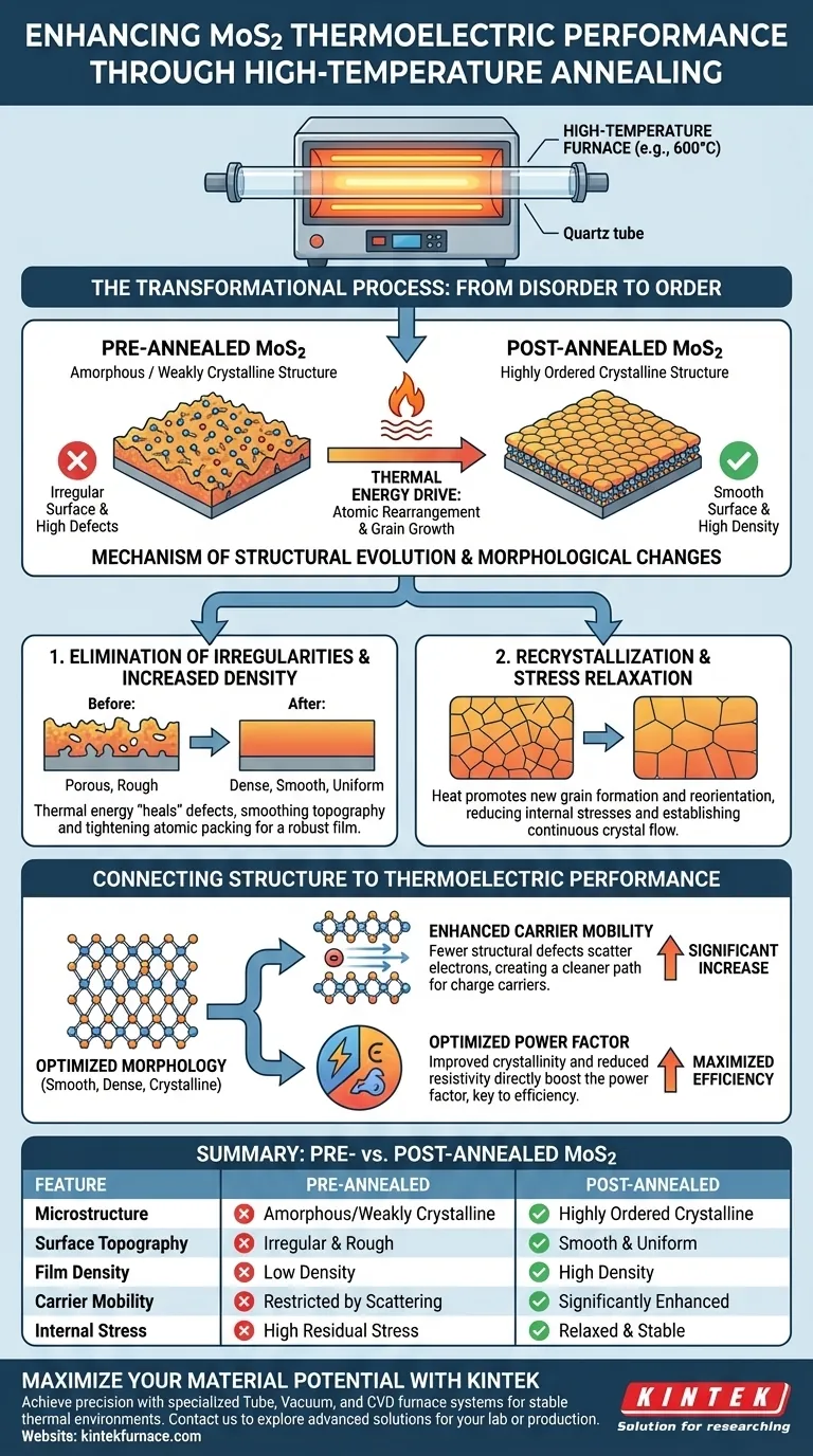
The annealing process modifies MoS2 morphology by leveraging high thermal energy to drive atomic rearrangement and grain growth. This transformation eliminates irregular surface microstructures, resulting in a significantly smoother and denser thin film.
Core Takeaway Thermal processing converts Molybdenum Disulfide films from an amorphous or weakly crystalline state into a highly ordered structure. This morphological refinement reduces electron scattering, directly enhancing carrier mobility and the power factor, which are the defining metrics of thermoelectric efficiency.

The Mechanism of Structural Evolution
Thermal Energy and Atomic Rearrangement
In a high-temperature furnace, typically around 600°C, the thermal energy provided acts as a catalyst for structural change.
This energy forces the atoms within the MoS2 film to break free from their initial, often disordered positions.
Once mobilized, these atoms rearrange themselves into a more energetically stable, ordered lattice structure.
Recrystallization and Grain Growth
The process shifts the material from an amorphous or weakly crystalline state toward a robust crystalline phase.
Heat encourages the formation of new grains and allows existing grains to reorient.
This growth and reorientation are critical for reducing internal stresses and establishing a continuous crystal flow throughout the film.
Specific Morphological Changes
Elimination of Surface Irregularities
Before annealing, MoS2 films often exhibit irregular microstructures that can impede performance.
The annealing process effectively "heals" these defects, smoothing out the film's topography.
Increased Film Density
As grains grow and atoms settle into an ordered lattice, the overall packing of the material tightens.
This results in a denser thin film, which is structurally more robust than the pre-annealed precursor.
connecting Structure to Performance
Enhancing Carrier Mobility
The elimination of physical irregularities and the increase in surface smoothness create a "cleaner" path for charge carriers.
With fewer structural defects to scatter electrons, carrier mobility increases significantly.
Optimizing the Power Factor
The power factor is a composite metric essential for thermoelectric performance.
By optimizing the microscopic morphology—specifically through improved crystallinity and reduced resistivity—the annealing process directly boosts this power factor.
Understanding the Necessity of Control
The Importance of a Controlled Environment
While heat is the driver, the environment must be strictly regulated, often using a Quartz Tube Furnace.
Precise temperature control is required to facilitate recrystallization without degrading the material.
Managing Internal Stress
Proper annealing does not just grow grains; it relaxes the material.
The rearrangement of grains reduces the metal's internal stresses, preventing mechanical failures or cracks that could interrupt electrical continuity.
Making the Right Choice for Your Goal
To maximize the utility of annealing for your specific MoS2 application, consider the following:
- If your primary focus is Electrical Conductivity: Prioritize temperatures that maximize grain size and continuity to minimize resistivity.
- If your primary focus is Structural Integrity: Ensure the annealing schedule allows sufficient time for internal stress relaxation to prevent film cracking.
By strictly controlling the thermal evolution of the microstructure, you transform MoS2 from a disordered material into a high-performance thermoelectric component.
Summary Table:
| Feature | Pre-Annealed MoS2 | Post-Annealed MoS2 |
|---|---|---|
| Microstructure | Amorphous / Weakly Crystalline | Highly Ordered Crystalline |
| Surface Topography | Irregular & Rough | Smooth & Uniform |
| Film Density | Low Density | High Density |
| Carrier Mobility | Restricted by Scattering | Significantly Enhanced |
| Internal Stress | High Residual Stress | Relaxed & Stable |
Maximize Your Material Potential with KINTEK
Ready to achieve precision in your MoS2 thin film processing? Contact us today to explore our advanced solutions.
Backed by expert R&D and manufacturing, KINTEK offers specialized Tube, Vacuum, and CVD furnace systems designed to provide the stable thermal environments and precise temperature control necessary for optimal grain growth and stress relaxation. Whether you are conducting research or scaling production, our customizable high-temperature furnaces empower labs and industrial manufacturers to transform disordered materials into high-performance thermoelectric components. Let our expertise drive your success.
Visual Guide
References
- Irasani Rahayu, Melania Suweni Muntini. Effect of Annealing Techniques on the Thermoelectric Properties of Molybdenum Disulfide Thin Films Prepared by RF Sputtering. DOI: 10.1088/1742-6596/3139/1/012035
This article is also based on technical information from Kintek Furnace Knowledge Base .
Related Products
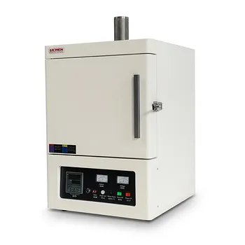
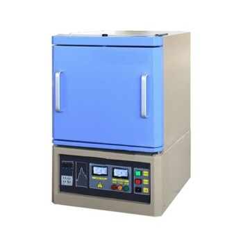
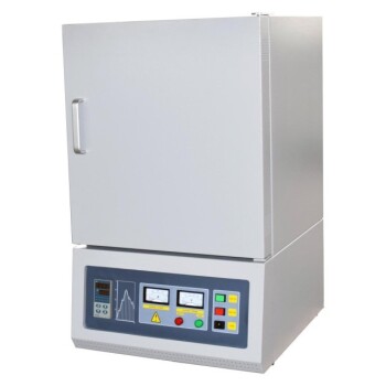
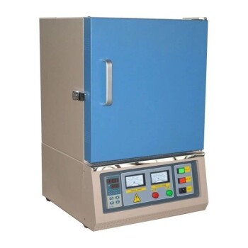
- Molybdenum Vacuum Heat Treat Furnace
- 1200℃ Muffle Oven Furnace for Laboratory
- 1700℃ Controlled Inert Nitrogen Atmosphere Furnace
- High Temperature Muffle Oven Furnace for Laboratory Debinding and Pre Sintering
- 1800℃ High Temperature Muffle Oven Furnace for Laboratory
People Also Ask
- What is one of the most important uses of vacuum heat treating furnaces in aerospace? Achieve Superior Strength in Aircraft Alloys
- How does vacuum heat treating work in terms of temperature and time control? Master Precise Material Transformations
- Why are vacuum heat treating furnaces essential for aerospace? Ensure Superior Material Integrity for High-Stakes Applications
- How does a vacuum heat treat furnace work? Achieve Pristine, High-Performance Results
- How does vacuum heat treating affect the grain structure of metal alloys? Achieve Precise Microstructure Control