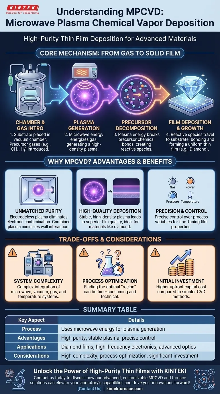
At its core, Microwave Plasma Chemical Vapor Deposition (MPCVD) is a process that uses focused microwave energy to transform gas into a plasma. This highly energized plasma then breaks down precursor gases into their fundamental components, which subsequently deposit onto a substrate to form a high-purity, uniform thin film.
MPCVD's primary advantage lies in its ability to generate a clean, dense, and stable plasma without direct electrode contact. This isolation is the key to creating exceptionally pure and high-quality films, making it a leading method for materials like synthetic diamond.
The Core Mechanism: From Gas to Solid Film
To understand how MPCVD works, it's best to break the process down into a sequence of controlled steps. Each stage is critical for achieving the final film characteristics.
Step 1: Chamber Preparation and Gas Introduction
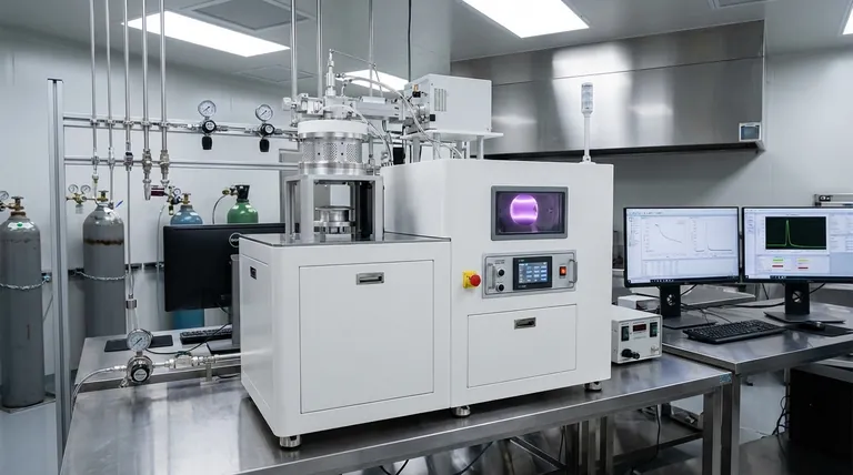
First, a substrate—the material to be coated—is placed inside a vacuum-sealed reaction chamber. The chamber is then evacuated to a very low pressure to remove any contaminants.
Next, a specific mixture of precursor gases is introduced into the chamber. For diamond deposition, this is typically a mix of a carbon source (like methane) and hydrogen.
Step 2: Plasma Generation via Microwaves
A microwave generator, often a magnetron, produces high-frequency microwave energy. This energy is guided into the reaction chamber.
The intense electromagnetic field from the microwaves energizes free electrons within the gas. These electrons oscillate violently, colliding with gas atoms and molecules.
Step 3: Precursor Decomposition
These energetic collisions transfer energy throughout the gas, knocking more electrons loose and causing widespread ionization. This process rapidly creates a high-density plasma, a superheated state of matter consisting of ions, electrons, and neutral species.
The intense energy within the plasma is sufficient to break the chemical bonds of the precursor gases, decomposing them into highly reactive species. For example, methane (CH₄) is broken down into carbon and hydrogen radicals.
Step 4: Film Deposition and Growth
These reactive species then travel to the surface of the heated substrate. There, they undergo chemical reactions that cause them to bond with the surface and with each other.
Layer by layer, these atoms build up on the substrate, forming a solid, crystalline, or amorphous thin film with precisely controlled properties.
Why MPCVD Is a Preferred Method
MPCVD is not just one of many options; its unique characteristics make it the superior choice for many demanding applications.
Unmatched Purity
Traditional plasma generation methods often use internal electrodes, which can erode during the process and contaminate the resulting film. MPCVD is electrodeless, generating the plasma with external microwave energy. This eliminates a major source of impurities.
Furthermore, the plasma is typically contained in the center of the chamber, preventing it from interacting with the chamber walls and further reducing contamination.
High-Quality Deposition
The process generates a very stable and high-density plasma. This allows for a higher concentration of reactive species, which can lead to faster deposition rates and superior film quality, particularly for difficult-to-grow materials like high-quality diamond.
Precision and Control
Operators have precise control over key variables like gas composition, pressure, microwave power, and substrate temperature. This allows for fine-tuning the film's thickness, crystalline structure, uniformity, and electronic properties.
Understanding the Trade-offs
While powerful, the MPCVD method has practical considerations that must be weighed against its benefits.
System Complexity
An MPCVD reactor is a complex piece of equipment. It integrates a microwave power source, waveguides, a high-vacuum system, sophisticated gas handling, and precise temperature control systems, all of which must work in harmony.
Process Optimization
Achieving the desired film properties requires careful and often time-consuming process development. Finding the optimal "recipe" of power, pressure, gas flow, and temperature for a specific application is a highly technical task.
Initial Investment
Due to their complexity and precision engineering, MPCVD systems typically represent a higher upfront capital investment compared to some simpler deposition techniques like basic thermal CVD.
Making the Right Choice for Your Goal
Selecting MPCVD depends entirely on the requirements of your final product.
- If your primary focus is ultimate purity and crystalline quality: MPCVD is the industry standard for applications like single-crystal diamond, high-frequency electronics, and advanced optics.
- If your primary focus is large-area uniformity for industrial production: MPCVD is highly scalable and provides the stable, uniform plasma necessary for coating large wafers or multiple parts simultaneously.
- If your primary focus is research and material exploration: The precise control afforded by MPCVD makes it an ideal tool for developing and characterizing new thin-film materials.
By leveraging contained microwave energy, MPCVD provides an unparalleled level of control and purity in the creation of advanced materials.
Summary Table:
| Key Aspect | Details |
|---|---|
| Process | Uses microwave energy to create plasma for gas decomposition and film deposition |
| Advantages | High purity, no electrode contamination, stable plasma, precise control |
| Applications | Diamond films, high-frequency electronics, advanced optics, research |
| Considerations | High system complexity, requires process optimization, significant initial investment |
Unlock the Power of High-Purity Thin Films with KINTEK!
Are you working on cutting-edge materials like synthetic diamond, high-frequency electronics, or advanced optics? KINTEK's advanced high-temperature furnace solutions, including our specialized CVD/PECVD systems, are designed to meet your exact needs. With exceptional R&D and in-house manufacturing, we offer deep customization to ensure your MPCVD processes deliver superior purity, uniformity, and performance. Don't let system complexity hold you back—let us help you optimize your deposition for faster results and higher quality.
Contact us today to discuss how our tailored solutions can elevate your laboratory's capabilities and drive your innovations forward!
Visual Guide
Related Products
- 915MHz MPCVD Diamond Machine Microwave Plasma Chemical Vapor Deposition System Reactor
- MPCVD Machine System Reactor Bell-jar Resonator for Lab and Diamond Growth
- Cylindrical Resonator MPCVD Machine System for Lab Diamond Growth
- Multi Heating Zones CVD Tube Furnace Machine for Chemical Vapor Deposition Equipment
- Inclined Rotary Plasma Enhanced Chemical Deposition PECVD Tube Furnace Machine
People Also Ask
- What are some key features and benefits of the microwave plasma chemical vapor deposition system? Achieve Unmatched Material Synthesis
- What is the MPCVD method and why is it considered effective for diamond deposition? Superior Purity & High Growth Rates
- What are the essential components of an MPCVD reactor system? Build a Pristine Environment for High-Purity Materials
- How does the MPCVD process work to deposit diamond? A Guide to High-Purity Synthesis
- What is the purpose of a microwave plasma chemical vapor deposition system? Grow High-Purity Diamonds and Advanced Materials


