The interaction between sputtering systems and lift-off processes functions as an additive patterning cycle specifically designed to create high-quality electrical contacts without damaging sensitive underlying materials. In this workflow, the sputtering system deposits a blanket layer of conductive material (such as Tantalum/Gold) over a photolithographic mask, while the subsequent lift-off step removes the mask and the metal on top of it, leaving behind the precise electrode geometry needed for the device.
The synergy between sputtering and lift-off allows for the precise fabrication of high-conductivity coplanar waveguides. This interaction is critical for enabling the efficient injection of RF currents required for the high-sensitivity detection of orbital torques in ST-FMR measurements.
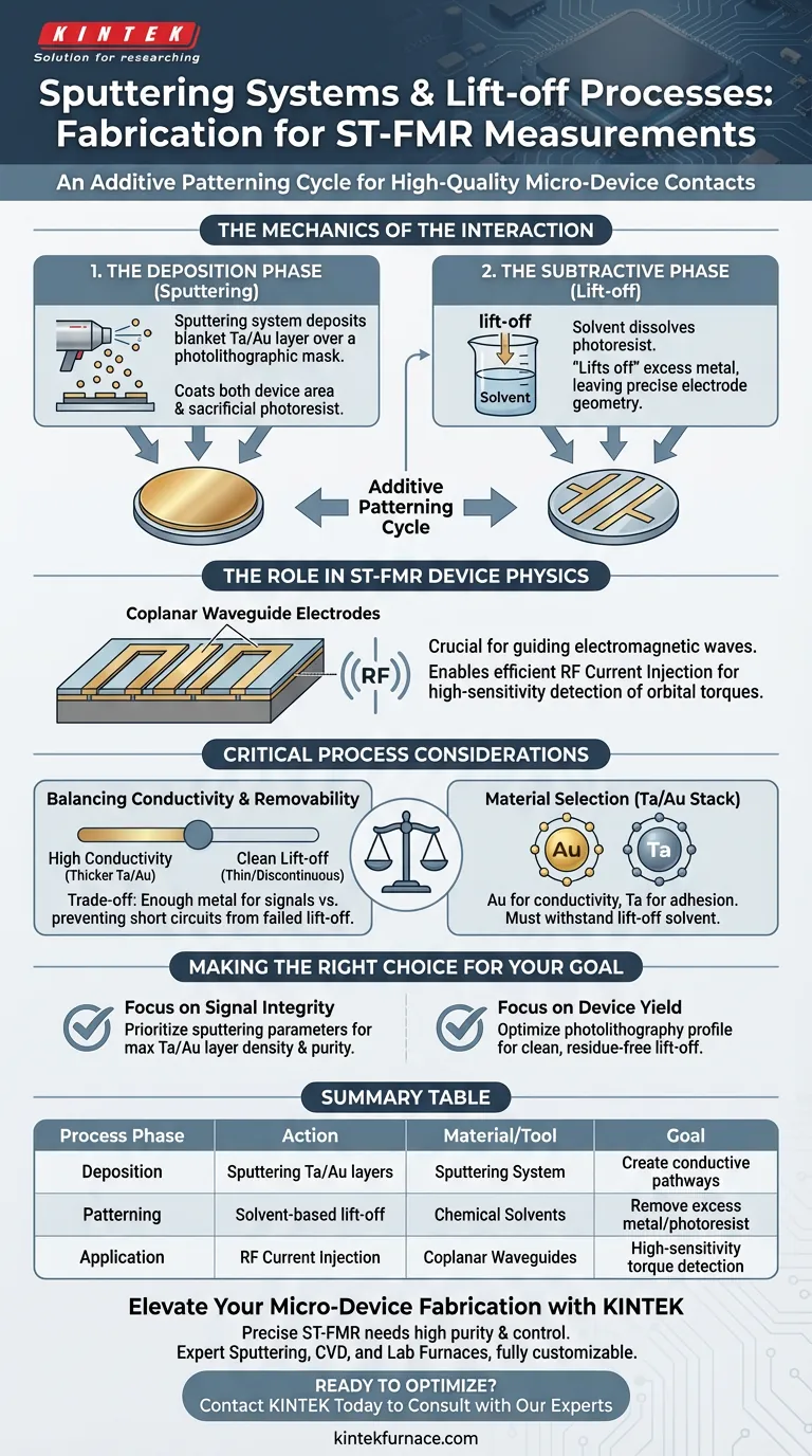
The Mechanics of the Interaction
The Deposition Phase
The process begins with the sputtering system, which is responsible for creating the conductive pathways.
This system deposits specific metal layers, identified in your context as Tantalum/Gold (Ta/Au).
This deposition occurs over a substrate that has already been patterned via photolithography, meaning the metal coats both the intended device area and the sacrificial photoresist.
The Subtractive Phase
The lift-off process serves as the shaping mechanism.
Once the metal deposition is complete, a solvent is used to dissolve the underlying photoresist.
As the resist dissolves, it "lifts off" the excess metal situated on top of it, leaving metal only where the resist was absent (the pattern).
The Role in ST-FMR Device Physics
Fabrication of Coplanar Waveguides
The primary output of this combined process is the creation of coplanar waveguide electrodes.
These structures are essential for guiding electromagnetic waves across the surface of the micro-device.
Enabling RF Current Injection
The quality of the sputtered film directly impacts the device's performance.
High-conductivity electrodes allow for the efficient injection of RF currents into the thin-film devices.
This efficiency is a prerequisite for the high-sensitivity detection of orbital torques, which is the ultimate goal of the ST-FMR measurement.
Critical Process Considerations
Balancing Conductivity and Removability
A key trade-off in this interaction involves the thickness and coverage of the sputtered metal.
You must deposit enough Ta/Au to ensure high conductivity for the RF signals.
However, if the sputtered layer is too continuous or thick, the lift-off process may fail to cleanly remove the excess metal, resulting in short circuits or geometric defects.
Material Selection
The choice of Ta/Au is strategic for this specific interaction.
Gold provides the necessary conductivity for the waveguide, while Tantalum typically acts as an adhesion layer.
This stack must withstand the chemical environment of the lift-off solvent without degrading.
Making the Right Choice for Your Goal
To optimize your ST-FMR device fabrication, align your process parameters with your specific measurement needs:
- If your primary focus is Signal Integrity: Prioritize the sputtering parameters to maximize the density and purity of the Ta/Au layer for the highest possible conductivity.
- If your primary focus is Device Yield: Focus on the photolithography profile to ensure the lift-off process can cleanly remove all excess metal without residue.
The successful integration of sputtering and lift-off is the foundational step that transforms raw materials into functional sensors capable of detecting precise orbital torques.
Summary Table:
| Process Phase | Action | Material/Tool Used | Goal |
|---|---|---|---|
| Deposition | Sputtering Ta/Au layers | Sputtering System | Create conductive pathways over photolithography |
| Patterning | Solvent-based lift-off | Chemical Solvents | Remove excess metal and sacrificial photoresist |
| Application | RF Current Injection | Coplanar Waveguides | High-sensitivity detection of orbital torques |
Elevate Your Micro-Device Fabrication with KINTEK
Precise ST-FMR measurements require the highest film purity and deposition control. At KINTEK, we understand the critical balance between conductivity and pattern resolution. Backed by expert R&D and manufacturing, we offer a comprehensive range of high-performance systems including Sputtering, CVD, and Lab High-Temp Furnaces (Muffle, Tube, Rotary, and Vacuum), all fully customizable to meet your unique research needs.
Ready to optimize your thin-film deposition and lift-off yields?
Contact KINTEK Today to Consult with Our Experts
Visual Guide
References
- Ke Tang, Seiji Mitani. Enhanced orbital torque efficiency in nonequilibrium Ru50Mo50(0001) alloy epitaxial thin films. DOI: 10.1063/5.0195775
This article is also based on technical information from Kintek Furnace Knowledge Base .
Related Products
- Spark Plasma Sintering SPS Furnace
- HFCVD Machine System Equipment for Drawing Die Nano Diamond Coating
- RF PECVD System Radio Frequency Plasma Enhanced Chemical Vapor Deposition
- Cylindrical Resonator MPCVD Machine System for Lab Diamond Growth
- Custom Made Versatile CVD Tube Furnace Chemical Vapor Deposition CVD Equipment Machine
People Also Ask
- What is the significance of high-precision temperature monitoring systems in SPS? Control Ti-6Al-4V/HA Microstructure
- What is the function of sintering furnaces? Transform Powders into Dense, Strong Components
- What are the advantages of spark plasma sintering (SPS) over traditional forging? Precision Microstructural Control
- What are the advantages of using a Spark Plasma Sintering (SPS) furnace? Achieve Rapid Densification and High ZT
- What is unique about the heating mechanism of a Spark Plasma Sintering (SPS) furnace when preparing nanostructured h-BN ceramics? Achieve Ultra-Fast Densification and Suppress Grain Growth


