High-vacuum thermal evaporation is strictly required to ensure the deposition of a pure, highly conductive gold electrode by minimizing gas particle interference. This system creates an extremely low-pressure environment that allows gold atoms to travel in a straight line—a long "mean free path"—directly to the device surface without scattering or oxidizing.
The high-vacuum environment is the defining factor in preventing impurity inclusions, ensuring the gold electrode forms a high-quality ohmic contact with the hole transport layer for maximum device efficiency.
The Physics of Vacuum Deposition
Maximizing the Mean Free Path
In a standard atmosphere, gas molecules are densely packed. If you attempted to evaporate gold in these conditions, the gold atoms would immediately collide with air molecules and scatter.
A high-vacuum system removes these obstacles. It allows gold atoms to travel with a long mean free path, ensuring directional deposition onto the target substrate.
Precision Control
This method allows for the creation of specific layer thicknesses, such as the standard 80 nm gold electrode referenced in high-performance designs.
Operating at pressures as low as 4 x 10⁻⁶ Torr provides the meticulous control necessary to achieve precise energy level alignment within the device stack.
Ensuring Material Purity and Conductivity
Eliminating Contamination
The most critical role of the vacuum is preventing the inclusion of impurity atoms.
Oxygen, moisture, and other environmental gases can degrade the metal or the underlying sensitive perovskite layers. The vacuum chamber isolates the process, ensuring that only pure gold is deposited.
Superior Electrical Conductivity
Because the deposited layer is free from oxides and contaminants, the resulting electrode exhibits superior electrical conductivity.
This low resistance is vital for the solar cell to extract current efficiently without losing energy as heat at the back contact.
Optimizing the Device Interface
High-Quality Ohmic Contact
For a perovskite solar cell to function correctly, the back electrode must form an ohmic contact with the hole transport layer (HTL).
Thermal evaporation ensures a clean interface that facilitates easy charge transfer. A contaminated interface would create a Schottky barrier, impeding charge flow and lowering the cell's voltage and fill factor.
Mechanical Adhesion
The kinetic energy of the gold atoms arriving at the substrate in a vacuum promotes strong physical adhesion.
This ensures the 80 nm layer remains mechanically stable, preventing delamination that would lead to immediate device failure.
Understanding the Trade-offs
Equipment Complexity and Cost
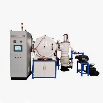
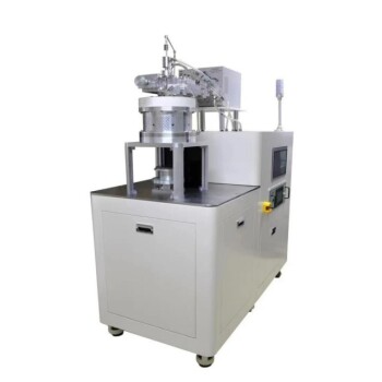
Achieving high vacuum requires sophisticated pumping systems (often turbomolecular pumps) and robust stainless steel chambers.
This makes the fabrication process significantly more expensive and energy-intensive compared to non-vacuum methods like screen printing.
Low Material Utilization
Thermal evaporation is a "line-of-sight" process.
Gold radiates in all directions from the source, meaning a significant amount of expensive metal coats the chamber walls rather than the solar cell, leading to high material waste.
Making the Right Choice for Your Goal
While alternative methods exist, high-vacuum thermal evaporation remains the gold standard for high-efficiency research devices.
- If your primary focus is Maximum Efficiency: Prioritize high-vacuum evaporation to ensure the lowest possible contact resistance and a pristine ohmic contact.
- If your primary focus is Cost Reduction: Be aware that this method incurs higher capital and material costs due to waste, despite its superior performance.
Ultimately, the high-vacuum environment is the non-negotiable price for achieving the purity and interface quality required for top-tier perovskite performance.
Summary Table:
| Feature | High-Vacuum Thermal Evaporation | Benefit for Perovskite Cells |
|---|---|---|
| Mean Free Path | Long (minimal gas collisions) | Directional deposition and uniform thickness |
| Purity Level | Extremely high (low impurity atoms) | Superior electrical conductivity & low resistance |
| Interface Quality | Clean, oxide-free contact | High-quality ohmic contact with HTL |
| Thickness Control | Nanometer precision (e.g., 80 nm) | Optimized energy level alignment |
| Pressure Range | Typically < 4 x 10⁻⁶ Torr | Prevents oxidation and contamination |
Maximize Your Solar Cell Efficiency with KINTEK
Precision matters in thin-film deposition. KINTEK provides industry-leading vacuum solutions designed specifically for high-stakes research and manufacturing. Backed by expert R&D and manufacturing, KINTEK offers a full range of Muffle, Tube, Rotary, Vacuum, and CVD systems, all fully customizable to meet your unique laboratory requirements.
Whether you need to achieve the perfect ohmic contact for perovskite solar cells or require high-purity material deposition, our thermal evaporation and high-temp furnace systems deliver the control you need.
Ready to upgrade your fabrication process? Contact KINTEK today to discuss your custom furnace needs!
References
- Seyyedeh Sedigheh Azad, Iraj Mohammadpoor‐Baltork. Stability enhancement of perovskite solar cells using multifunctional inorganic materials with UV protective, self cleaning, and high wear resistance properties. DOI: 10.1038/s41598-024-57133-8
This article is also based on technical information from Kintek Furnace Knowledge Base .
Related Products
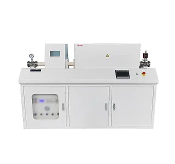
- Slide PECVD Tube Furnace with Liquid Gasifier PECVD Machine
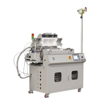
- Custom Made Versatile CVD Tube Furnace Chemical Vapor Deposition CVD Equipment Machine
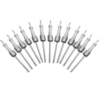
- Ultra Vacuum Electrode Feedthrough Connector Flange Power Lead for High Precision Applications
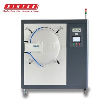
- Vacuum Heat Treat Furnace with Ceramic Fiber Liner
- 2200 ℃ Graphite Vacuum Heat Treat Furnace
People Also Ask
- What is PECVD specification? A Guide to Choosing the Right System for Your Lab
- How is silicon dioxide deposited from tetraethylorthosilicate (TEOS) in PECVD? Achieve Low-Temperature, High-Quality SiO2 Films
- What are the classifications of CVD based on vapor characteristics? Optimize Your Thin Film Deposition Process
- How does chemical vapour deposition (CVD) differ from PVD? Key Differences in Thin-Film Coating Methods
- What are the drawbacks of CVD compared to PECVD? Key Limitations for Your Lab
