At its core, Chemical Vapor Deposition (CVD) is the foundational manufacturing process used to build the essential, ultra-thin layers that constitute modern electronic components. It involves depositing solid materials from a gas onto a substrate, allowing for the creation of pure, uniform films that form the building blocks of transistors, capacitors, and integrated circuits.
The true significance of CVD lies not just in what it does, but in the atomic-level precision it enables. This control over thickness, purity, and composition is the critical factor that allows for the fabrication of complex, high-performance nanoscale devices that power all modern electronics.
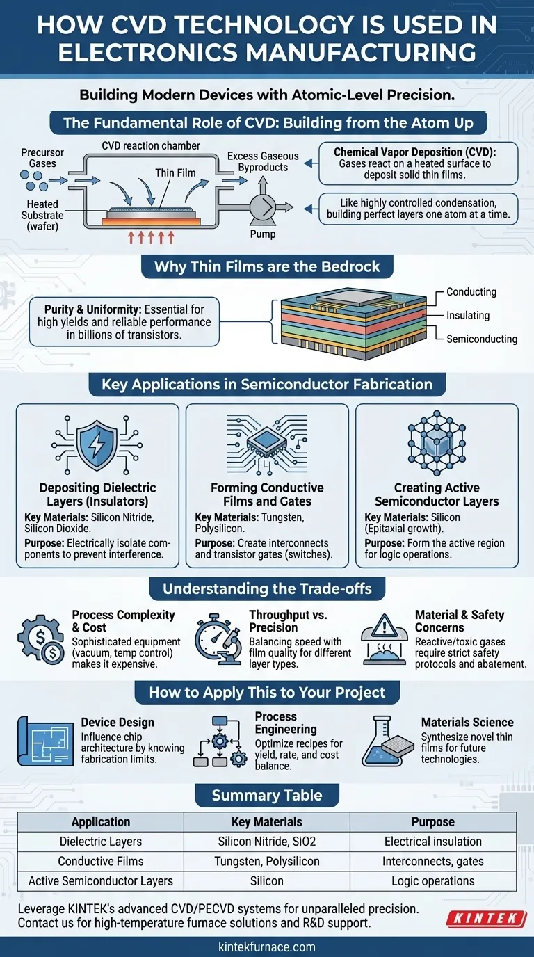
The Fundamental Role of CVD: Building from the Atom Up
To grasp why CVD is indispensable, you must think of modern chips not as single objects, but as microscopic cities with billions of structures. CVD is the primary construction method used to build these structures layer by layer.
What is Chemical Vapor Deposition?
CVD is a process where a substrate, such as a silicon wafer, is placed in a reaction chamber. Precursor gases containing the desired elements are introduced into the chamber.
These gases react or decompose on the heated surface of the substrate, leaving behind a solid thin film of the intended material. The excess gaseous byproducts are then pumped out.
Think of it as a highly controlled form of condensation, where specific molecules are precisely "rained" down to form a perfect, solid layer one atom at a time.
Why Thin Films are the Bedrock of Electronics
A modern microprocessor is a three-dimensional structure made of stacked layers of conducting, insulating, and semiconducting materials. Each layer must have a precise thickness and specific electrical properties.
CVD is the technology used to deposit these critical layers. Whether it's an insulating layer to prevent a short circuit or a conductive layer to form a wire, CVD provides the required control.
The Importance of Purity and Uniformity
In a device with billions of transistors, a single atomic impurity or a slight variation in a film's thickness can cause a catastrophic failure.
CVD excels at producing high-purity and highly uniform films across the entire surface of a wafer. This consistency is non-negotiable for achieving high yields and reliable device performance.
Key Applications in Semiconductor Fabrication
CVD is not one single process but a family of techniques used to deposit different materials, each serving a distinct purpose within the semiconductor device.
Depositing Dielectric Layers (Insulators)
Materials like silicon nitride and silicon dioxide are deposited via CVD to act as insulators. These layers electrically isolate different conductive components, preventing signals from interfering with one another, which is essential in a densely packed integrated circuit.
Forming Conductive Films and Gates
CVD is used to deposit metal films (like tungsten) that serve as the microscopic "wiring" or interconnects between transistors. It is also used to deposit polycrystalline silicon (polysilicon), a key material for creating the "gate" of a transistor, which acts as the switch that turns it on or off.
Creating Active Semiconductor Layers
The most fundamental layer is often the semiconductor itself. Epitaxial CVD processes are used to grow perfectly ordered silicon crystals on the wafer. This pristine layer forms the active region of the transistor where all the processing and logic operations actually occur.
Understanding the Trade-offs
While powerful, CVD is a complex and resource-intensive technology with inherent trade-offs that engineers must manage.
Process Complexity and Cost
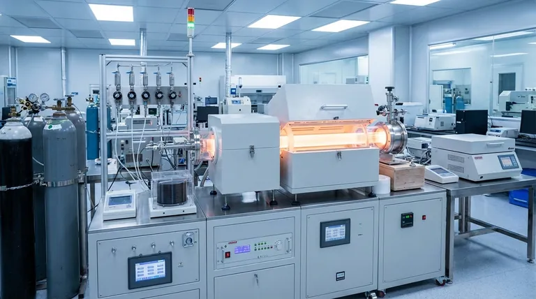
CVD systems are sophisticated machines that require high vacuum, precise temperature control, and complex gas delivery systems. This makes the equipment expensive to purchase and operate.
Throughput vs. Precision
There is often a trade-off between the speed of deposition and the quality of the film. Faster CVD processes might be used for thicker, less critical layers, while slower, more precise methods are reserved for the most sensitive components of a device.
Material and Safety Concerns
The precursor gases used in CVD are often highly reactive, toxic, or flammable. This necessitates significant investment in safety protocols, handling infrastructure, and abatement systems to neutralize waste gas.
How to Apply This to Your Project
Understanding the function and constraints of CVD is crucial for anyone involved in the electronics value chain.
- If your primary focus is device design: Knowing the capabilities of CVD informs what is physically possible to fabricate, influencing the architecture of next-generation chips.
- If your primary focus is process engineering: Your goal is to optimize CVD recipes to balance film quality, deposition rate, and cost to maximize manufacturing yield and device performance.
- If your primary focus is materials science: CVD is a primary tool for synthesizing and testing novel thin films with new electronic, optical, or physical properties that could enable future technologies.
Ultimately, understanding Chemical Vapor Deposition is understanding the fundamental language in which modern electronic devices are written.
Summary Table:
| Application | Key Materials | Purpose |
|---|---|---|
| Dielectric Layers | Silicon Nitride, Silicon Dioxide | Electrical insulation to prevent interference |
| Conductive Films | Tungsten, Polysilicon | Forming interconnects and transistor gates |
| Active Semiconductor Layers | Silicon | Creating active regions for logic operations |
Leverage KINTEK's advanced CVD/PECVD systems and deep customization capabilities to achieve unparalleled precision in your electronics manufacturing. Our high-temperature furnace solutions, including Muffle, Tube, Rotary, and Vacuum & Atmosphere Furnaces, are designed to meet unique experimental needs with exceptional R&D support. Contact us today to enhance your lab's efficiency and innovation!
Visual Guide
Related Products
- Custom Made Versatile CVD Tube Furnace Chemical Vapor Deposition CVD Equipment Machine
- Split Chamber CVD Tube Furnace with Vacuum Station CVD Machine
- Multi Heating Zones CVD Tube Furnace Machine for Chemical Vapor Deposition Equipment
- Slide PECVD Tube Furnace with Liquid Gasifier PECVD Machine
- Controlled Inert Nitrogen Hydrogen Atmosphere Furnace
People Also Ask
- What future trends are expected in the development of CVD tube furnaces? Discover Smarter, More Versatile Systems
- What are the key application fields of CVD tube furnaces? Unlock Precision in Thin-Film Synthesis
- What improvements can be made to the bonding force of gate dielectric films using a CVD tube furnace? Enhance Adhesion for Reliable Devices
- What is a CVD tube furnace and what is its primary function? Discover Precision Thin-Film Deposition
- What temperature range do standard CVD tube furnaces operate at? Unlock Precision for Your Material Deposition


