The primary plasma methods used in Chemical Vapor Deposition (CVD) are Plasma-Enhanced CVD (PECVD), Microwave Plasma-Assisted CVD (MPCVD), Remote Plasma-Enhanced CVD (RPECVD), and Low-Energy Plasma-Enhanced CVD (LEPECVD). These techniques leverage the energy of a plasma to drive chemical reactions, allowing for high-quality film deposition at significantly lower temperatures than traditional thermal CVD processes.
The core reason for using plasma in CVD is to decouple the energy source for chemical reactions from thermal heat. By using an electrically-generated plasma to create reactive gas species, deposition can occur at low temperatures, protecting thermally sensitive substrates from damage.
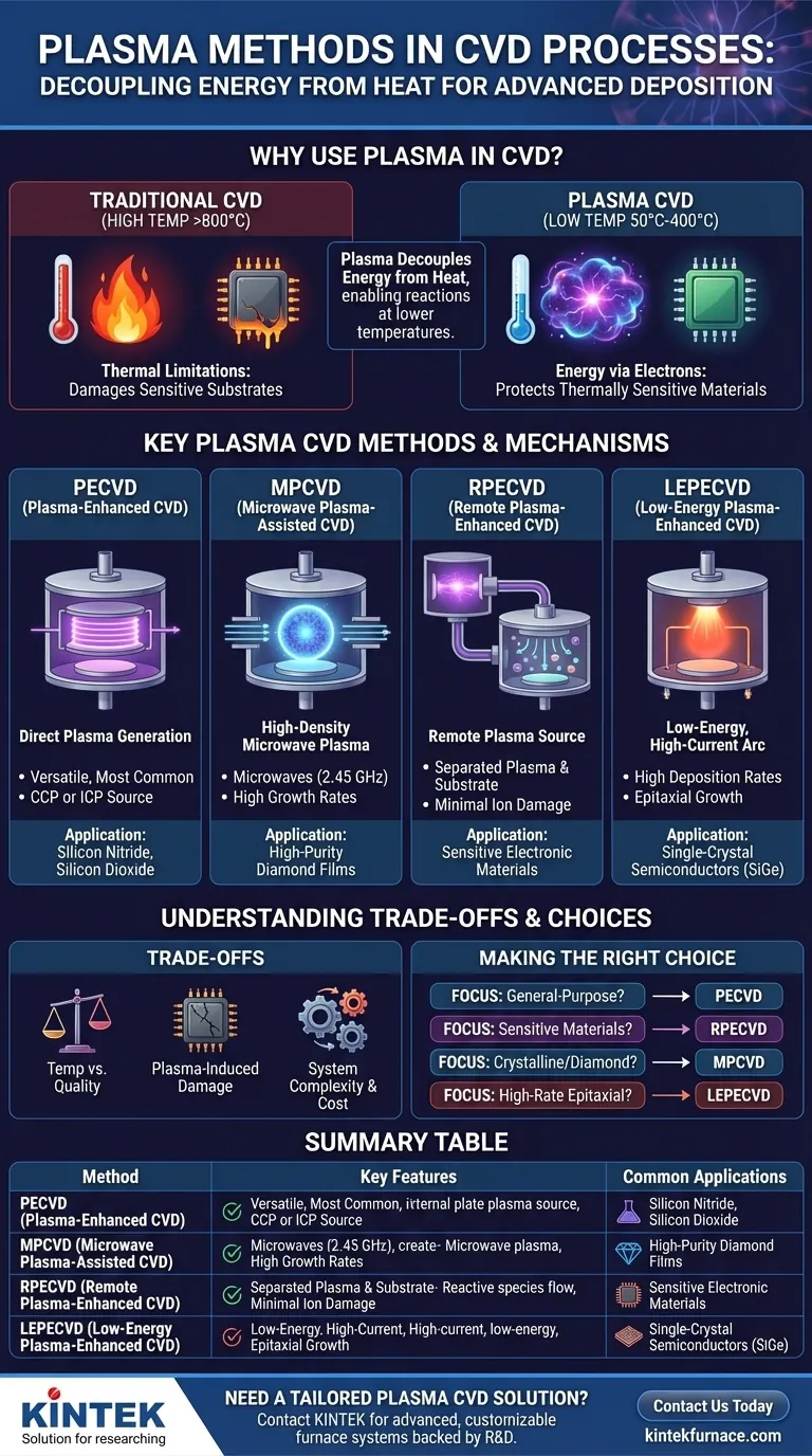
Why Use Plasma in CVD?
Traditional CVD relies on high temperatures (often >800°C) to provide the activation energy needed for precursor gases to react and form a solid film. The introduction of plasma fundamentally changes this energy dynamic.
Overcoming Thermal Limitations
Many advanced materials, such as polymers, certain semiconductors, or fully fabricated integrated circuits, cannot withstand the high temperatures of conventional CVD. Exposing them to such heat would cause them to melt, warp, or degrade.
Plasma provides an alternative energy pathway. It allows for the deposition of high-quality, durable films onto these sensitive substrates without causing thermal damage.
How Plasma Provides the Energy
A plasma is a partially ionized gas containing a mix of neutral particles, ions, electrons, and highly reactive free radicals. Within the CVD chamber, an electric field energizes free electrons, which then collide with neutral gas molecules.
These collisions break the molecules apart, creating the chemically reactive species needed for deposition. Because the energy is delivered by energetic electrons rather than heat, the overall process can be run at much lower temperatures, typically from 50°C to 400°C.
A Breakdown of Key Plasma CVD Methods
While all plasma CVD techniques share the same fundamental principle, they differ in how the plasma is generated and controlled. This distinction has significant implications for the resulting film properties and suitable applications.
Plasma-Enhanced CVD (PECVD)
PECVD is the most common and versatile plasma deposition technique. The plasma is generated directly within the deposition chamber, with the substrate immersed in it.
This is typically achieved using a capacitively coupled plasma (CCP) or an inductively coupled plasma (ICP). PECVD is a workhorse technology for depositing materials like silicon nitride (SiN) and silicon dioxide (SiO₂) in semiconductor manufacturing.
Microwave Plasma-Assisted CVD (MPCVD)
MPCVD uses microwaves (typically at 2.45 GHz) to generate a very high-density plasma. This high concentration of reactive species enables high growth rates and the formation of high-quality crystalline materials.
Its most notable application is the synthesis of high-purity diamond films, which is difficult to achieve with other CVD methods.
Remote Plasma-Enhanced CVD (RPECVD)
In RPECVD, the plasma is generated in a separate chamber and the reactive species are then flowed into the main deposition chamber where the substrate is located.
The primary advantage is that the substrate is not in direct contact with the most energetic parts of the plasma. This dramatically reduces damage from ion bombardment, making RPECVD ideal for depositing films on extremely sensitive electronic materials.
Low-Energy Plasma-Enhanced CVD (LEPECVD)
LEPECVD is a specialized variant that focuses on producing high-quality, single-crystal films, particularly for semiconductors like silicon-germanium (SiGe).
It uses a low-voltage, high-current arc discharge to create a plasma with a high density of ions but very low ion energy. This combination allows for high deposition rates while minimizing crystalline defects in the growing film.
Understanding the Trade-offs
Using plasma introduces powerful new capabilities, but it also brings a new set of process variables and potential challenges that must be managed.
Temperature vs. Film Quality
While low-temperature processing is the key benefit of plasma CVD, films deposited at lower temperatures can sometimes have lower density or higher hydrogen content compared to their high-temperature thermal CVD counterparts. Process optimization is critical to matching the film quality requirements.
Plasma-Induced Damage
In direct plasma methods like PECVD, energetic ions can be accelerated toward the substrate, potentially causing physical damage or creating defects in the film. This is the primary problem that techniques like RPECVD are designed to solve by separating the plasma source from the substrate.
System Complexity and Cost
Plasma CVD systems are inherently more complex than simple thermal CVD furnaces. They require vacuum systems, gas handling, RF or microwave power generators, and impedance matching networks, which increases their cost and maintenance requirements.
Making the Right Choice for Your Application
Selecting the correct plasma CVD method depends entirely on the material you are depositing and the characteristics of your substrate.
- If your primary focus is general-purpose deposition on robust substrates: Standard PECVD offers the best balance of performance, flexibility, and cost for common dielectric films.
- If your primary focus is depositing on extremely sensitive electronic materials: RPECVD is the superior choice, as it is specifically designed to minimize plasma-induced damage.
- If your primary focus is growing high-purity crystalline films like diamond: MPCVD is the industry standard due to its ability to generate the required high-density plasma.
- If your primary focus is high-rate, epitaxial semiconductor growth: LEPECVD provides a unique capability for creating high-quality crystalline layers with minimal defects.
Ultimately, choosing the right plasma technique is about matching the tool's specific energy delivery mechanism to the demands of your material and substrate.
Summary Table:
| Plasma CVD Method | Key Features | Common Applications |
|---|---|---|
| PECVD | Direct plasma generation, versatile | Silicon nitride, silicon dioxide in semiconductors |
| MPCVD | High-density plasma, high growth rates | High-purity diamond films |
| RPECVD | Remote plasma, minimal substrate damage | Sensitive electronic materials |
| LEPECVD | Low ion energy, high deposition rates | Single-crystal semiconductors like SiGe |
Need a tailored plasma CVD solution for your lab? At KINTEK, we specialize in advanced high-temperature furnace systems, including CVD/PECVD setups, backed by exceptional R&D and in-house manufacturing. Our deep customization capabilities ensure precise alignment with your unique experimental needs, whether you're working with sensitive substrates or demanding high-purity films. Contact us today to enhance your deposition processes and achieve superior results!
Visual Guide
Related Products
- Custom Made Versatile CVD Tube Furnace Chemical Vapor Deposition CVD Equipment Machine
- Split Chamber CVD Tube Furnace with Vacuum Station CVD Machine
- Multi Heating Zones CVD Tube Furnace Machine for Chemical Vapor Deposition Equipment
- Slide PECVD Tube Furnace with Liquid Gasifier PECVD Machine
- Controlled Inert Nitrogen Hydrogen Atmosphere Furnace
People Also Ask
- What is the working principle of a CVD tube furnace? Achieve Precise Thin Film Deposition for Your Lab
- Which industries and research fields benefit from CVD tube furnace sintering systems for 2D materials? Unlock Next-Gen Tech Innovations
- Why are CVD tube furnace sintering systems indispensable for 2D material research and production? Unlock Atomic-Scale Precision
- What are the key application fields of CVD tube furnaces? Unlock Precision in Thin-Film Synthesis
- What customization options are available for CVD tube furnaces? Tailor Your System for Superior Material Synthesis


