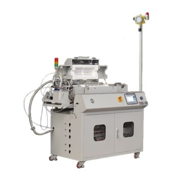
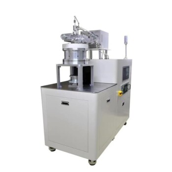
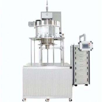
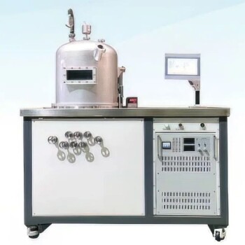
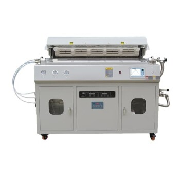
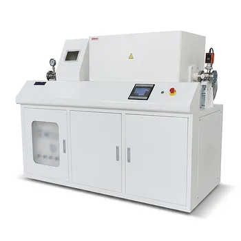
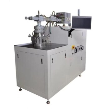
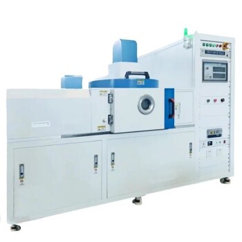
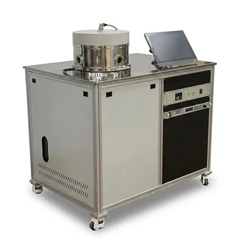
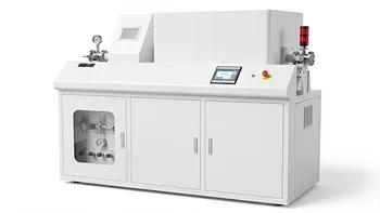
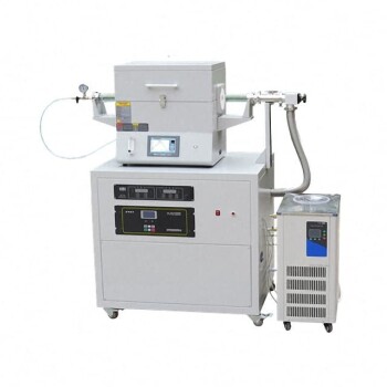
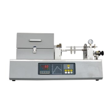
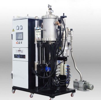
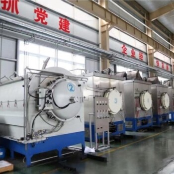
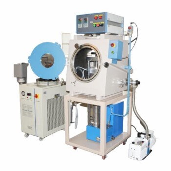
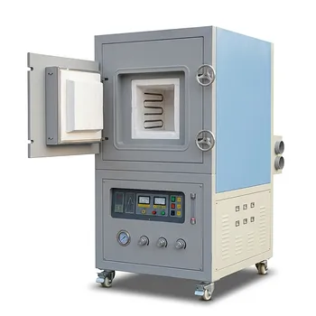
LPCVD is the primary method for depositing high-performance silicon nitride (Si3N4) passivation layers in graphene sensor fabrication.
By operating at reduced pressures, Low Pressure Chemical Vapor Deposition (LPCVD) equipment enables the growth of a dense, approximately 200 nm thick insulating film on silicon substrates. This layer serves as a critical dielectric barrier, ensuring that the graphene sensor remains electrically isolated and chemically stable when exposed to high-temperature and high-pressure (HTHP) environments.
Core Takeaway: LPCVD equipment is essential for creating a stoichiometrically stable and dense passivation layer that protects graphene sensors. Its ability to provide superior step coverage and film uniformity at the sub-atmospheric level is what makes it the standard for high-reliability sensor manufacturing.
Superior Material Properties for Sensor Protection
High Film Density and Stoichiometric Stability
LPCVD allows for the growth of silicon nitride (Si3N4) with extremely high film density. This density is crucial because it creates a robust barrier against moisture and ionic contaminants that could otherwise degrade the sensor's performance.
The process ensures stoichiometric stability, meaning the chemical composition of the film remains consistent throughout the layer. This stability is vital for maintaining predictable electrical insulation performance over the long-term life of the sensor.
Superior Step Coverage
In sensor architecture, substrates often have complex topographies or "steps." LPCVD equipment excels at step coverage, ensuring that the passivation layer wraps uniformly around these structures without thinning at the edges.
This uniform coverage prevents "weak spots" in the insulation. Without it, the graphene sensor would be prone to electrical leakage or short-circuiting in high-stress environments.
The Role of Reduced Pressure in Film Quality
Minimizing Gas-Phase Reactions
LPCVD operates at sub-atmospheric pressures, which significantly increases the mean free path of gas molecules. This environment reduces unwanted gas-phase reactions that typically lead to particle contamination in other deposition methods.
By minimizing these reactions, the equipment ensures a cleaner, more uniform film growth across the entire surface of the wafer. This is a critical requirement for precision semiconductor manufacturing and high-sensitivity graphene applications.
Enhanced Film Uniformity
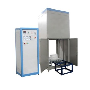
The reduced pressure in an LPCVD tube furnace facilitates a more controlled delivery of precursor gases like silane and ammonia. This results in exceptional thickness uniformity, which is essential for maintaining consistent sensor characteristics across large batches.
This uniformity is why LPCVD is favored for multi-wafer furnace tools, allowing manufacturers to produce high volumes of graphene sensors with identical passivation specs.
Understanding the Trade-offs
The Thermal Budget Constraint
LPCVD is typically a high-temperature process, often operating near or above 800°C to 1000°C. While this heat is necessary for high-quality Si3N4 growth, it can be a limiting factor if other sensor components or substrates cannot withstand high thermal loads.
If a project involves temperature-sensitive materials already integrated into the device, engineers must carefully sequence the deposition to avoid damaging the active sensor elements.
Process Complexity and Speed
While LPCVD provides superior film quality, it often involves slower deposition rates compared to Plasma Enhanced CVD (PECVD). The need for high-vacuum systems and precise gas-flow ratios also increases the complexity of the equipment maintenance.
However, for graphene sensors where long-term reliability is the priority, the trade-off of a slower, more complex process is usually justified by the resulting film's durability.
Implementing LPCVD in Your Sensor Workflow
Strategic Application Based on Goals
When integrating an LPCVD step into your graphene sensor production, the choice of parameters depends heavily on the final application of the device.
- If your primary focus is extreme environment durability: Prioritize the maximum density of the Si3N4 layer by utilizing higher temperatures and longer dwell times.
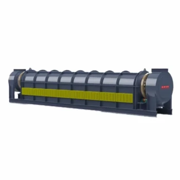
- If your primary focus is high-volume manufacturing: Leverage horizontal tube LPCVD systems to ensure maximum wafer-to-wafer uniformity across large batches.
- If your primary focus is minimizing substrate stress: Carefully control the cooling rates post-deposition to manage the thermal expansion mismatch between the silicon nitride and the silicon substrate.
By leveraging the precise control offered by LPCVD equipment, you can ensure that your graphene sensors are shielded by a passivation layer capable of withstanding the most demanding industrial conditions.
Summary Table:
| Feature | Benefit for Graphene Sensors | Impact on Performance |
|---|---|---|
| High Film Density | Robust barrier against moisture and ions | Ensures long-term chemical stability |
| Superior Step Coverage | Uniform coating over complex structures | Prevents electrical leakage and shorts |
| Stoichiometric Stability | Consistent chemical composition | Provides predictable dielectric properties |
| Reduced Pressure | Minimal gas-phase particle contamination | Results in cleaner, high-uniformity films |
| Thermal Precision | High-quality Si3N4 growth | Maximum durability in HTHP environments |
Elevate Your Sensor Fabrication with KINTEK’s Precision LPCVD Solutions
High-performance graphene sensors require the uncompromising quality that only advanced thermal processing can provide. KINTEK specializes in high-temperature laboratory furnaces and consumables designed to meet the rigorous demands of semiconductor and sensor research.
Our extensive range of equipment includes:
- Advanced CVD & LPCVD Systems for superior film uniformity.
- Tube, Vacuum, and Atmosphere Furnaces for controlled environments.
- Customizable High-Temp Solutions tailored to your specific material constraints.
Whether you are scaling up production or perfecting a niche sensor application, KINTEK provides the reliability and technical expertise you need to succeed. Contact us today to discuss your project and get a custom quote!
References
- Simei Zeng, Tao Deng. A Novel High-Temperature Pressure Sensor Based on Graphene Coated by Si<sub>3</sub>N<sub>4</sub>. DOI: 10.1109/jsen.2022.3232626
This article is also based on technical information from Kintek Furnace Knowledge Base .
Related Products
- Custom Made Versatile CVD Tube Furnace Chemical Vapor Deposition CVD Equipment Machine
- MPCVD Machine System Reactor Bell-jar Resonator for Lab and Diamond Growth
- 915MHz MPCVD Diamond Machine Microwave Plasma Chemical Vapor Deposition System Reactor
- HFCVD Machine System Equipment for Drawing Die Nano Diamond Coating
- Multi Heating Zones CVD Tube Furnace Machine for Chemical Vapor Deposition Equipment
People Also Ask
- What is a CVD tube furnace and what is its primary function? Discover Precision Thin-Film Deposition
- Why are CVD tube furnace sintering systems indispensable for 2D material research and production? Unlock Atomic-Scale Precision
- How does CVD tube furnace sintering enhance graphene growth? Achieve Superior Crystallinity and High Electron Mobility
- Which industries and research fields benefit from CVD tube furnace sintering systems for 2D materials? Unlock Next-Gen Tech Innovations
- What temperature range do standard CVD tube furnaces operate at? Unlock Precision for Your Material Deposition