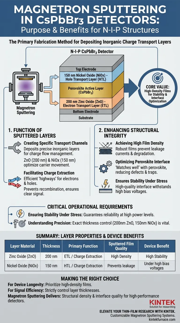
Magnetron sputtering acts as the primary fabrication method for depositing inorganic charge transport layers within N-I-P type CsPbBr3 detector structures. Specifically, this equipment is used to deposit a 200 nm Zinc Oxide (ZnO) layer and a 150 nm Nickel Oxide (NiOx) layer. These layers are critical for the efficient extraction and transport of electrons and holes, directly influencing the detector's sensitivity and response speed.
The core value of using magnetron sputtering lies in its ability to create high-density films that interface perfectly with the perovskite layer, ensuring the device remains stable even when subjected to high bias voltages.
The Function of Sputtered Layers
Creating Specific Transport Channels
The primary function of the equipment is to deposit precise inorganic layers that manage the flow of electrical current.
In this specific N-I-P architecture, it builds a ZnO layer (approximately 200 nm thick) and a NiOx layer (approximately 150 nm thick). These specific thicknesses are targeted to optimize the movement of charge carriers.
Facilitating Charge Extraction
The deposited layers serve as the functional "highways" for electrons and holes generated within the detector.
By utilizing magnetron sputtering, these inorganic materials are engineered to efficiently extract charges from the active region, preventing recombination and ensuring a clear signal.
Enhancing Structural Integrity
Achieving High Film Density
A distinct advantage of magnetron sputtering in this context is the physical quality of the deposited material.
The process results in high-density films, which are far more robust than layers produced by some alternative deposition methods. This density is essential for preventing leakage currents and structural degradation.
Optimizing the Perovskite Interface
The sputtering process allows for a deposition that "matches well" with the underlying or overlying perovskite interface.
This compatibility is vital for reducing defects at the junction between layers, which often serve as traps for charge carriers and reduce overall efficiency.
Critical Operational Requirements
Ensuring Stability Under Stress
The ultimate goal of using this specific equipment is to guarantee the detector's reliability under operational stress.
Because the sputtered films are dense and the interface is high-quality, the device maintains stability under high bias voltages. This capability is essential for detectors that must operate at higher power levels without breaking down.
Understanding the Precision Required
While magnetron sputtering offers superior film quality, it requires exact control over layer thickness to function correctly.
If the ZnO layer deviates significantly from 200 nm, or the NiOx from 150 nm, the balance of electron and hole transport may be disrupted. The equipment is therefore not just for "coating," but for achieving a specific geometric and electronic architecture necessary for the N-I-P structure to function.
Making the Right Choice for Your Goal
When evaluating the fabrication process for CsPbBr3 detectors, consider your primary performance objectives:
- If your primary focus is Device Longevity: Prioritize magnetron sputtering to achieve the high-density films required to withstand high bias voltages without degradation.
- If your primary focus is Signal Efficiency: Ensure your process strictly controls the thickness of the ZnO (200 nm) and NiOx (150 nm) layers to optimize charge extraction.
Magnetron sputtering provides the necessary structural density and interface quality to transform raw perovskite materials into high-performance, stable detectors.
Summary Table:
| Layer Material | Thickness | Primary Function |
|---|---|---|
| Zinc Oxide (ZnO) | 200 nm | Electron Transport Layer (ETL) / Charge Extraction |
| Nickel Oxide (NiOx) | 150 nm | Hole Transport Layer (HTL) / Charge Extraction |
| Sputtered Film Quality | High Density | Prevents leakage current & improves structural integrity |
| Device Benefit | High Stability | Ensures performance under high bias voltages |
Elevate Your Thin-Film Research with KINTEK
Precision in layer thickness and film density is the key to high-performance perovskite detectors. Backed by expert R&D and manufacturing, KINTEK offers cutting-edge Magnetron Sputtering systems, alongside our Muffle, Tube, Rotary, Vacuum, and CVD systems—all customizable for your unique lab requirements.
Whether you are optimizing ZnO/NiOx transport layers or developing advanced N-I-P architectures, our equipment provides the control you need for superior results.
Contact KINTEK today to discuss your customized fabrication solutions!
Visual Guide
References
- Jincong Pang, Guangda Niu. Reconfigurable perovskite X-ray detector for intelligent imaging. DOI: 10.1038/s41467-024-46184-0
This article is also based on technical information from Kintek Furnace Knowledge Base .
Related Products
- 915MHz MPCVD Diamond Machine Microwave Plasma Chemical Vapor Deposition System Reactor
- Multi Heating Zones CVD Tube Furnace Machine for Chemical Vapor Deposition Equipment
- Slide PECVD Tube Furnace with Liquid Gasifier PECVD Machine
- Cylindrical Resonator MPCVD Machine System for Lab Diamond Growth
- Custom Made Versatile CVD Tube Furnace Chemical Vapor Deposition CVD Equipment Machine
People Also Ask
- How does the MPCVD process work to deposit diamond? A Guide to High-Purity Synthesis
- What factors influence the quality of diamond deposition in the MPCVD method? Master the Critical Parameters for High-Quality Diamond Growth
- In which industries is the microwave plasma chemical vapor deposition system commonly used? Unlock High-Purity Material Synthesis
- What are some key features and benefits of the microwave plasma chemical vapor deposition system? Achieve Unmatched Material Synthesis
- What are the essential components of an MPCVD reactor for diamond film deposition? Unlock High-Quality Diamond Growth


