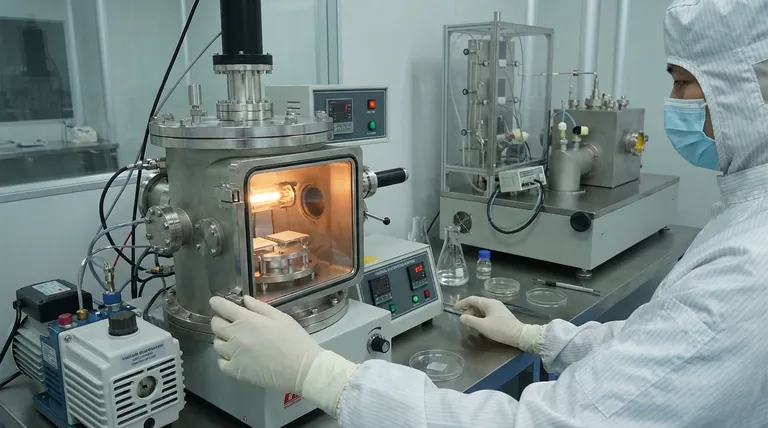
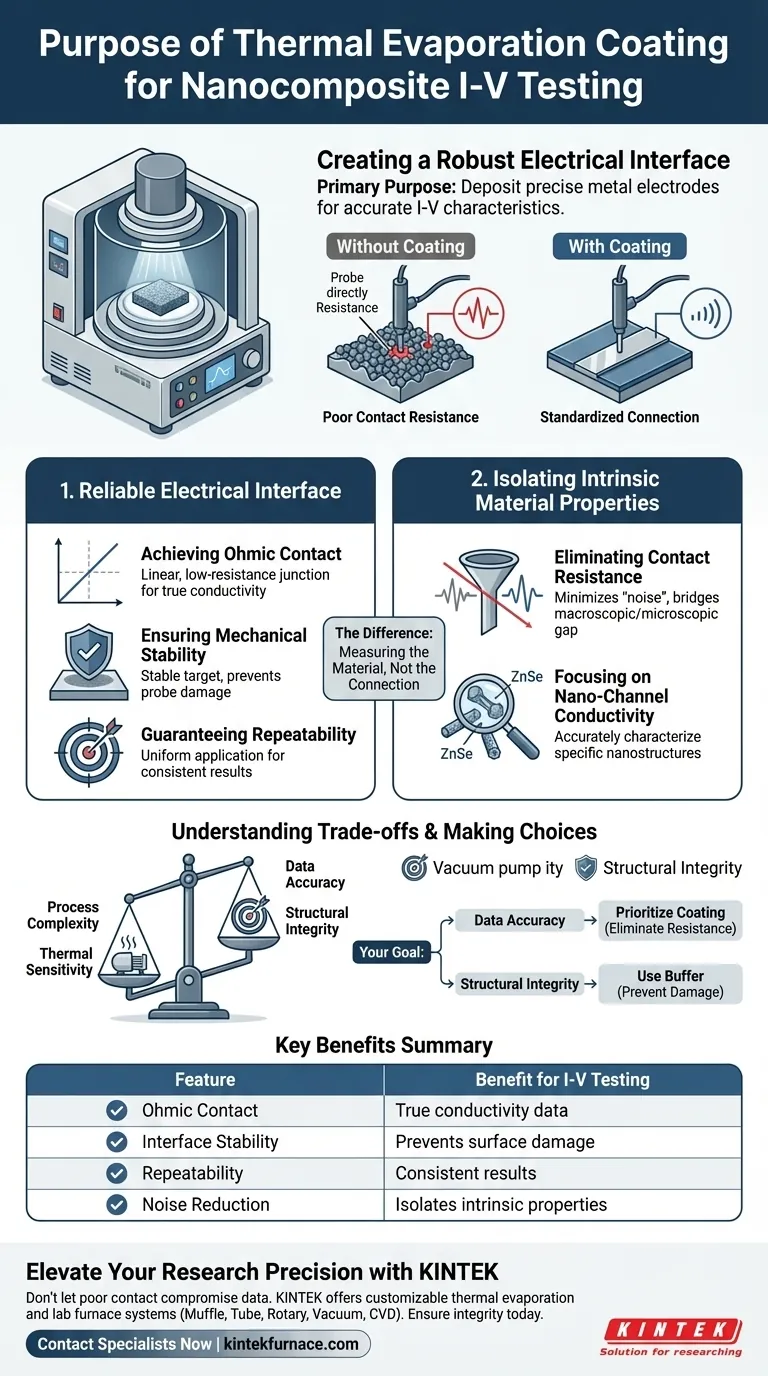
The primary purpose of using a thermal evaporation coating system is to deposit precise metal electrodes, such as copper, onto the surface of a nanocomposite material prior to testing. This step creates a robust electrical interface that is essential for capturing accurate current-voltage (I-V) characteristics.
By standardizing the connection points, this process ensures that the measured electrical signals represent the true conductivity of the material, rather than artifacts caused by poor contact resistance.
Creating a Reliable Electrical Interface
Achieving Ohmic Contact
The most critical function of the coating is to establish proper ohmic contact. Without a deposited electrode, the interface between the testing probe and the nanocomposite acts as a barrier.
Thermal evaporation creates a linear, low-resistance junction. This ensures that the current flows freely according to Ohm's Law, rather than being impeded by a rectifying (diode-like) contact.
Ensuring Mechanical Stability
Directly probing a nanomaterial can be physically inconsistent. The deposited metal layer provides a mechanically stable target for testing instruments.
This prevents the probes from shifting or damaging the delicate surface of the nanocomposite during the measurement process.
Guaranteeing Repeatability
Scientific data must be reproducible to be valid. Thermal evaporation applies the electrode material uniformly across the sample.
This repeatability ensures that subsequent tests yield consistent results, eliminating the variability often associated with manual probe placement on uneven surfaces.
Isolating Intrinsic Material Properties
Eliminating Contact Resistance
A major challenge in testing nanomaterials is contact resistance, which acts as "noise" in your data. If the contact is poor, the device measures the resistance of the connection rather than the sample.
The coating minimizes this interference. It bridges the gap between the macroscopic testing equipment and the microscopic surface.
Focusing on Nano-Channel Conductivity
The ultimate goal is to measure the specific behavior of the internal structures, such as Zinc Selenide (ZnSe) nano-channels.
By removing external variables, the thermal evaporation coating allows you to isolate and accurately characterize the conductivity of these specific nanostructures.
Understanding the Trade-offs
Process Complexity
While effective, thermal evaporation requires a high-vacuum environment. This adds a layer of complexity and time to the sample preparation process compared to simple mechanical probing.
Thermal Sensitivity
The process involves heating a source material until it evaporates. You must ensure your nanocomposite substrate can withstand the radiant heat and the heat of condensation during deposition without degrading.
Making the Right Choice for Your Goal
To get the most out of your I-V characterization, consider your specific testing objectives:
- If your primary focus is Data Accuracy: Prioritize this coating step to eliminate contact resistance and ensure the signal reflects the true material properties.
- If your primary focus is Structural Integrity: Use the coating to create a protective buffer, preventing sharp probes from physically damaging the nano-channels.
Proper electrode deposition is the difference between measuring a connection and measuring the material itself.
Summary Table:
| Feature | Benefit for I-V Testing |
|---|---|
| Ohmic Contact | Ensures linear, low-resistance current flow for true conductivity data. |
| Interface Stability | Provides a robust mechanical target for probes, preventing surface damage. |
| Repeatability | Guarantees uniform electrode application for consistent, reproducible results. |
| Noise Reduction | Eliminates contact resistance to isolate intrinsic material properties. |
Elevate Your Research Precision with KINTEK
Don’t let poor contact resistance compromise your data. Backed by expert R&D and manufacturing, KINTEK offers high-performance thermal evaporation and lab high-temp furnace systems—including Muffle, Tube, Rotary, Vacuum, and CVD systems—all fully customizable to meet your unique nanocomposite testing needs.
Ensure the integrity of your I-V characteristics today. Contact our specialists now to find the perfect coating solution for your lab!
Visual Guide
References
- Aiman Akylbekovа, Anatoli I. Popov. Annealing Effect on Structural, Optical and Electrophysical Properties of ZnSe Nanocrystals Synthesized into SiO2/Si Ion Track Template. DOI: 10.3390/ma17164149
This article is also based on technical information from Kintek Furnace Knowledge Base .
Related Products
- HFCVD Machine System Equipment for Drawing Die Nano Diamond Coating
- RF PECVD System Radio Frequency Plasma Enhanced Chemical Vapor Deposition
People Also Ask
- What is the advantage of using a CVD system for coating turbine blades? Master Complex Geometries with Ease
- What role does Chemical Vapor Deposition (CVD) equipment play in the surface coating of carbon fibers for composites?
- What is chemical vapor deposition (CVD) and its primary industrial application? Unlock Precision Thin Films for Electronics
- What materials are commonly used in CVD coating systems? Explore Key Materials for Superior Coatings
- What are the equipment for chemical vapor deposition? A Guide to the 5 Essential Components

