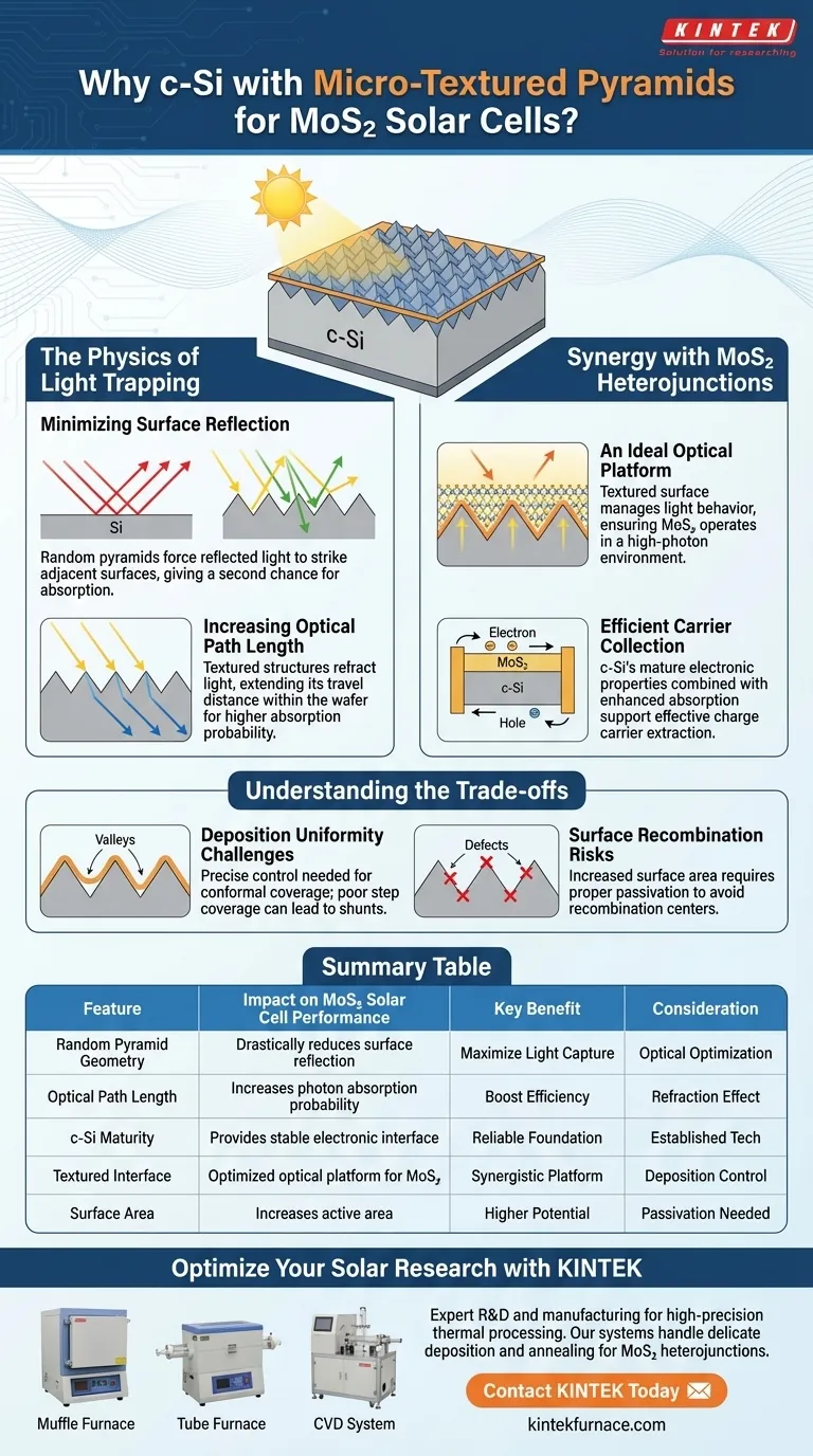
Crystalline silicon (c-Si) wafers serve as the foundational standard for MoS2 heterojunction solar cells largely due to their mature and predictable semiconductor properties. However, the specific selection of wafers with micro-textured random pyramid structures is an optical engineering decision designed to drastically minimize the reflection of incident light. By utilizing this geometry, the substrate acts as a sophisticated light trap, extending the optical path length to maximize absorption and facilitate efficient carrier collection in the device.
The selection of this specific substrate is a balance of electronic stability and optical optimization; while the c-Si material provides the conductive foundation, the pyramid texture ensures that photons are captured rather than reflected, significantly boosting the cell's potential efficiency.
The Physics of Light Trapping
Minimizing Surface Reflection
The primary limitation of flat silicon surfaces is their natural tendency to reflect a significant portion of incoming sunlight.
The micro-textured random pyramid structure combats this by altering the angle of incidence. Instead of bouncing light directly away from the cell, the pyramid geometry forces reflected light to strike adjacent pyramids, giving the material a second chance to absorb the photon.
Increasing Optical Path Length
Absorption is not just about getting light into the cell; it is about keeping it there long enough to generate energy.
These textured structures refract light at oblique angles, causing it to travel diagonally through the wafer rather than straight through. This effectively increases the optical path length, ensuring that photons interact with more semiconductor material, which significantly improves the probability of absorption.
Synergy with MoS2 Heterojunctions
An Ideal Optical Platform
The interaction between the bulk silicon and the thin MoS2 layer relies heavily on how light is managed at the interface.
The primary reference notes that this textured surface provides an ideal optical platform for the subsequent deposition of MoS2 layers. By managing light behavior at the substrate level, the device ensures that the MoS2 layer operates in a high-photon environment.
Efficient Carrier Collection
Beyond optics, the substrate architecture plays a role in the electrical performance of the cell.
The established maturity of c-Si wafers ensures a high-quality electronic interface. When combined with the enhanced absorption from the texture, the system supports efficient carrier collection, allowing the charge carriers generated by the light to be extracted effectively.
Understanding the Trade-offs
Deposition Uniformity Challenges
While optically superior, textured surfaces present a fabrication challenge compared to flat wafers.
Depositing a uniform layer of MoS2 over a complex, three-dimensional landscape of random pyramids requires precise process control. Poor step coverage (coating the valleys and peaks unevenly) can lead to electrical shunts or breaks in the heterojunction interface.
Surface Recombination Risks
Texturing increases the total surface area of the wafer significantly.
Without proper passivation, this increased surface area can introduce more surface defects. These defects can act as recombination centers, trapping charge carriers before they are collected, which would counteract the gains made in optical efficiency.
Making the Right Choice for Your Design
- If your primary focus is maximizing short-circuit current (Jsc): Utilize micro-textured random pyramid structures to exploit the "light trapping" effect and increased optical path length.
- If your primary focus is fabrication simplicity: Acknowledge that achieving conformal coverage of MoS2 on textured surfaces requires more advanced deposition techniques than on planar substrates.
By combining the electronic maturity of c-Si with the optical superiority of pyramid texturing, you create a robust platform optimized for high-performance energy conversion.
Summary Table:
| Feature | Impact on MoS2 Solar Cell Performance |
|---|---|
| Random Pyramid Geometry | Drastically reduces surface reflection by redirecting incident light. |
| Optical Path Length | Increases photon absorption probability via oblique light refraction. |
| c-Si Maturity | Provides a stable, high-quality electronic interface for carrier collection. |
| Textured Interface | Serves as an optimized optical platform for thin-film MoS2 deposition. |
| Surface Area | Increases active area but requires careful passivation to avoid recombination. |
Optimize Your Solar Research with KINTEK
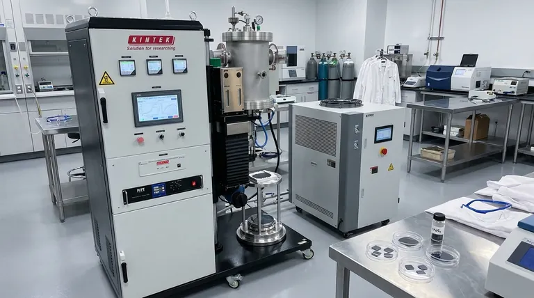
Transitioning from theoretical physics to high-performance energy devices requires the right thermal processing equipment. Backed by expert R&D and manufacturing, KINTEK offers high-precision Muffle, Tube, Rotary, Vacuum, and CVD systems designed to handle the delicate deposition and annealing needs of MoS2 heterojunctions.
Whether you are managing uniform layer growth on micro-textured c-Si wafers or developing next-generation lab scale prototypes, our customizable high-temperature furnaces provide the stability your project demands.
Ready to elevate your lab's capabilities?
Contact KINTEK Today to discuss your unique research requirements with our technical team.
Visual Guide
References
- Sel Gi Ryu, Keunjoo Kim. Photoenhanced Galvanic Effect on Carrier Collection of the MOS<sub>2</sub> Contact Layer in Silicon Solar Cells. DOI: 10.1002/pssa.202500039
This article is also based on technical information from Kintek Furnace Knowledge Base .
Related Products
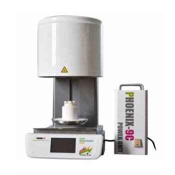
- Chairside Dental Porcelain Zirconia Sintering Furnace with Transformer for Ceramic Restorations
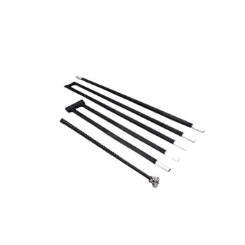
- Silicon Carbide SiC Thermal Heating Elements for Electric Furnace
People Also Ask
- What type of heating elements are preferred for zirconia sintering and why? Choose SiC or MoSi2 for Optimal Results
- What features contribute to the efficiency of a zirconia sintering furnace? Boost Lab Productivity with Advanced Systems
- How to select a zirconia sintering furnace supplier? Ensure Precision and Reliability for Your Lab
- Why is a zirconia sintering furnace considered essential for dental laboratories and clinics? Unlock Precision and Durability
- How do conventional vs rapid sintering in dental furnaces affect zirconia? Optimize Efficiency Without Sacrificing Strength