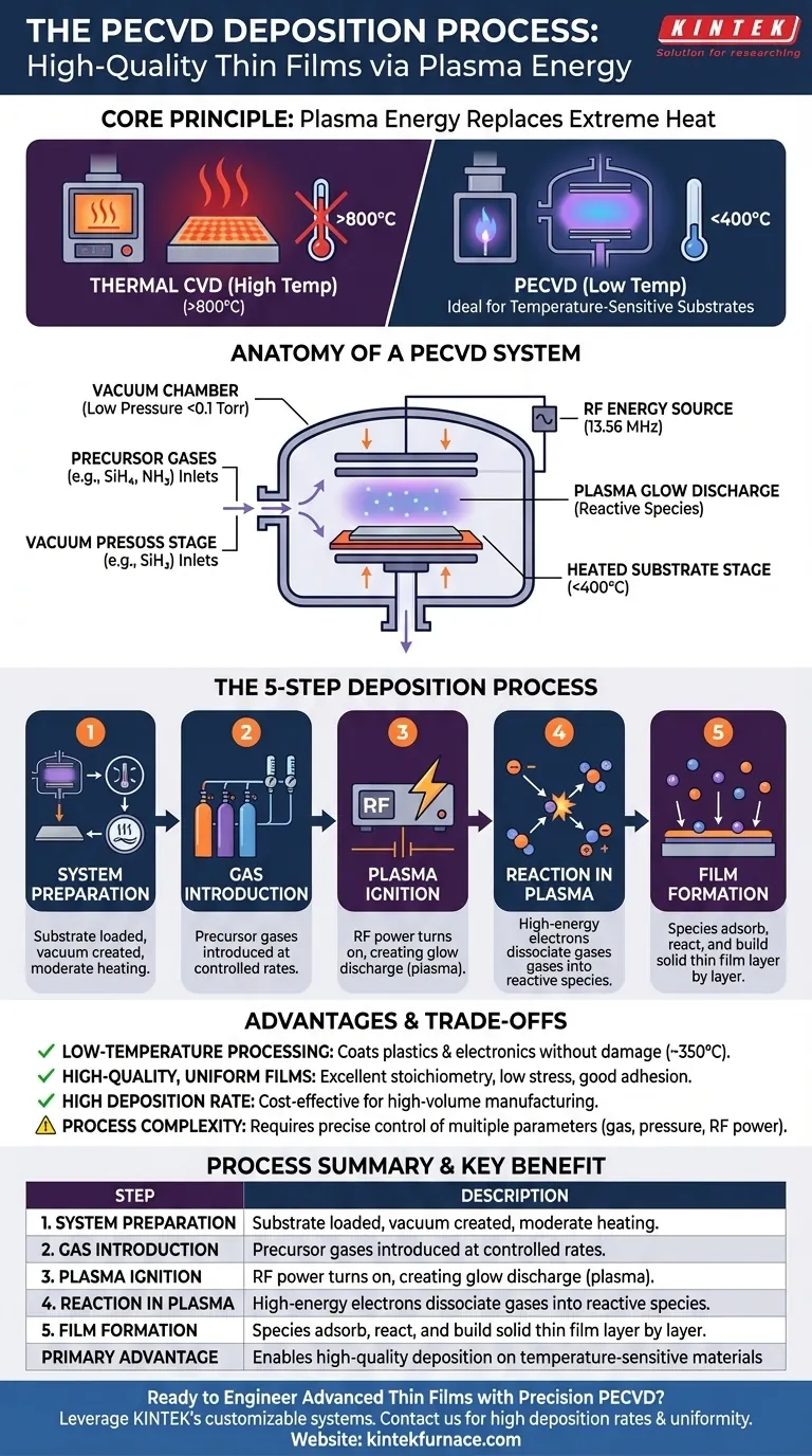
At its core, Plasma-Enhanced Chemical Vapor Deposition (PECVD) is a process that uses an energized gas, or plasma, to deposit high-quality thin films onto a surface. Unlike purely thermal methods that require extreme heat, PECVD uses the energy from plasma to initiate chemical reactions, allowing the deposition to occur at significantly lower temperatures.
The central principle of PECVD is substituting the intense heat of traditional deposition with the energy of a plasma. This fundamental shift enables the creation of uniform, low-stress films on substrates that cannot survive high-temperature environments.
The Anatomy of a PECVD System
To understand the process, you must first understand the environment where it occurs. A PECVD system is a precisely controlled environment built around a few key components.
The Vacuum Chamber
The entire process takes place inside a sealed vacuum chamber. The air is pumped out to a very low pressure (often below 0.1 Torr) to remove unwanted particles and create a clean, controllable environment for the chemical reactions.
The Precursor Gases
Reactant gases, known as precursors, are the raw ingredients for the film. For example, silane (SiH4) and ammonia (NH3) might be used to create a silicon nitride film. These gases are introduced into the chamber through controlled inlets.
The Energy Source
An electric field, typically a Radio Frequency (RF) source operating at 13.56 MHz, is applied between two parallel electrodes within the chamber. This energy is not used to heat the chamber but to ignite and sustain the plasma.
The Substrate Stage
The material to be coated, called the substrate, rests on a stage inside the chamber. This stage is often heated to a moderate, controlled temperature (e.g., below 400°C) to promote surface reactions and improve film quality.
The Step-by-Step Deposition Process
The PECVD process unfolds in a precise sequence, transforming gas molecules into a solid film.
Step 1: System Preparation
First, the substrate is placed inside the chamber, which is then sealed and pumped down to a high vacuum. The substrate is then gently heated to the target process temperature.
Step 2: Gas Introduction
The precursor gases are introduced into the chamber at a controlled flow rate. These gases fill the space between the electrodes, surrounding the substrate.
Step 3: Plasma Ignition
The RF power source is turned on, applying a voltage across the electrodes. This electrical energy strips electrons from some gas molecules, creating a glow discharge—the visible evidence of a plasma.
Step 4: Reaction in the Plasma
Within the plasma, high-energy electrons (often 100-300 eV) collide with the neutral precursor gas molecules. These collisions are energetic enough to break the molecules apart, a process called dissociation, creating a mix of highly reactive species like ions, radicals, and atoms.
Step 5: Film Formation
These chemically reactive species travel to the substrate's surface. Once there, they adsorb (bind) to the surface, react with each other, and form a stable, solid thin film. This process repeats, building the film layer by layer from nanometers to even millimeters in thickness.
Understanding the Advantages and Trade-offs
PECVD is widely adopted because its unique approach offers significant benefits, but it's essential to understand the context.
Advantage: Low-Temperature Processing
This is the primary benefit of PECVD. By using plasma energy instead of thermal energy to drive reactions, deposition can occur at temperatures around 350°C. This makes it ideal for coating temperature-sensitive materials like plastics or complete electronic devices that would be damaged by high heat.
Advantage: High-Quality, Uniform Films
PECVD can produce films that are highly uniform across a large substrate with excellent stoichiometry (the correct ratio of chemical elements). The resulting films also typically exhibit low internal stress, which improves their mechanical stability and adhesion.
Advantage: High Deposition Rate
Compared to some other low-temperature techniques, PECVD can deposit material relatively quickly, making it a cost-effective and efficient choice for manufacturing environments.
Consideration: Process Complexity
The quality of the final film depends on a careful balance of multiple parameters: gas flow rates, chamber pressure, substrate temperature, and RF power. Adjusting plasma density and energy is critical for controlling the film's microstructure, requiring a sophisticated level of process control.
Making the Right Choice for Your Application
Choosing a deposition method depends entirely on your project's constraints and desired outcomes.
- If your primary focus is depositing on temperature-sensitive substrates: PECVD is the definitive choice over conventional high-temperature CVD.
- If your primary focus is manufacturing efficiency: The combination of high deposition rates and uniform film quality makes PECVD extremely attractive for high-volume production.
- If your primary focus is fine-tuning film properties: PECVD offers a powerful set of control levers (gas chemistry, plasma energy) to precisely regulate the film's density, stress, and composition.
Ultimately, mastering PECVD is about leveraging plasma energy to engineer high-performance materials from the atom up.
Summary Table:
| Key PECVD Process Step | Description |
|---|---|
| 1. System Preparation | Substrate is placed in a vacuum chamber, which is pumped down and heated to a moderate temperature (e.g., <400°C). |
| 2. Gas Introduction | Precursor gases (e.g., SiH4, NH3) are introduced into the chamber at controlled flow rates. |
| 3. Plasma Ignition | An RF power source ignites a plasma, creating a glow discharge of highly energetic species. |
| 4. Reaction in Plasma | High-energy electrons dissociate gas molecules, creating reactive ions and radicals. |
| 5. Film Formation | Reactive species adsorb to the substrate surface, reacting to form a solid, uniform thin film layer by layer. |
| Primary Advantage | Enables high-quality deposition on temperature-sensitive materials like plastics and electronics. |
Ready to Engineer Advanced Thin Films with Precision PECVD?
Leveraging exceptional R&D and in-house manufacturing, KINTEK provides diverse laboratories with advanced high-temperature furnace solutions, including our sophisticated PECVD Systems. Our strong deep customization capability allows us to precisely tailor systems to meet your unique experimental requirements, whether you are working with delicate electronics, polymers, or other temperature-sensitive substrates.
Contact us today using the form below to discuss how our PECVD technology can enhance your research or production process with high deposition rates, excellent film uniformity, and low-stress results.
Visual Guide
Related Products
- Slide PECVD Tube Furnace with Liquid Gasifier PECVD Machine
- RF PECVD System Radio Frequency Plasma Enhanced Chemical Vapor Deposition
- Inclined Rotary Plasma Enhanced Chemical Deposition PECVD Tube Furnace Machine
- Inclined Rotary Plasma Enhanced Chemical Deposition PECVD Tube Furnace Machine
- Multi Heating Zones CVD Tube Furnace Machine for Chemical Vapor Deposition Equipment
People Also Ask
- What are the disadvantages of tube furnace cracking when processing heavy raw materials? Avoid Costly Downtime and Inefficiency
- What are the typical conditions for plasma-enhanced CVD processes? Achieve Low-Temperature Thin Film Deposition
- How does PECVD equipment contribute to TOPCon bottom cells? Mastering Hydrogenation for Maximum Solar Efficiency
- In which industries is the tube furnace commonly used? Essential for Materials Science, Energy, and More
- What is plasma in the context of PECVD? Unlock Low-Temperature Thin Film Deposition


