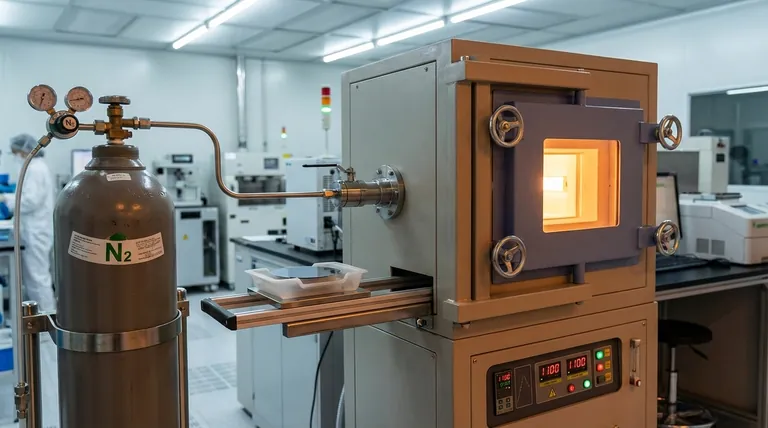
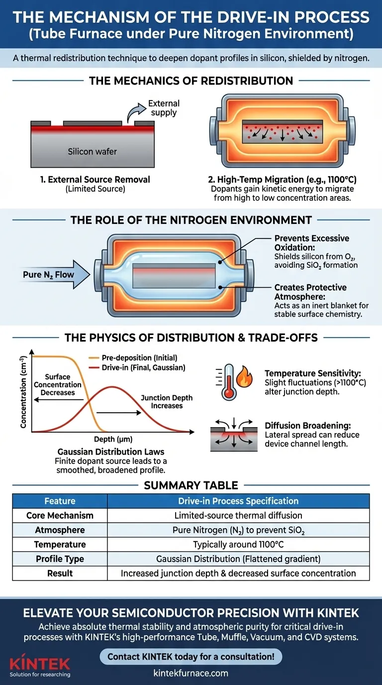
The drive-in process is a thermal redistribution technique executed after the external dopant source has been removed from the silicon wafer. By subjecting the wafer to high temperatures (typically around 1100°C) within a pure nitrogen atmosphere, the process forces previously introduced dopant atoms to diffuse deeper into the silicon substrate without creating an oxide layer.
The core mechanism relies on converting a shallow, high-concentration surface layer into a deeper, strictly controlled profile governed by Gaussian distribution, using nitrogen to shield the silicon from oxidation during the thermal cycle.
The Mechanics of Redistribution
Removal of the External Source
Before the drive-in begins, the external supply of dopant atoms used in the previous step (pre-deposition) is removed.
This creates a "limited source" diffusion scenario. The total amount of dopant in the silicon remains constant; the atoms merely rearrange themselves.
High-Temperature Migration
The tube furnace is heated to elevated temperatures, such as 1100°C.
At this thermal energy level, the dopant atoms gain the kinetic energy required to move through the crystal lattice. They naturally migrate from areas of high concentration (the surface) to areas of low concentration (deep inside the wafer).
The Role of the Nitrogen Environment
Preventing Excessive Oxidation
The primary reference indicates that a pure nitrogen environment is critical to prevent the formation of silicon dioxide ($\text{SiO}_2$) on the wafer surface.
If oxygen were present at these temperatures, it would consume silicon to grow an oxide layer. This would alter the interface and potentially disturb the dopant distribution near the surface.
Creating a Protective Atmosphere
Nitrogen acts as an inert blanket, similar to how gases like argon are used to protect metals during thermal treatment.
This ensures that the chemical composition of the silicon surface remains stable while the internal physical changes (diffusion) occur.
The Physics of Distribution
Gaussian Distribution Laws
Because the dopant source is limited to what is already inside the wafer, the resulting concentration profile follows Gaussian distribution laws.
This mathematical model dictates that as the drive-in time increases, the surface concentration decreases while the junction depth increases.
Profile Flattening
The sharp concentration gradient created during the initial pre-deposition is smoothed out.
This results in a broader, more gradual transition between the doped region and the substrate, which is essential for the electrical characteristics of many semiconductor devices.
Understanding the Trade-offs
Temperature Sensitivity
The process is highly sensitive to temperature variations. Even slight fluctuations around 1100°C can significantly alter the final depth of the junction, requiring precise furnace control.
Diffusion Broadening
While the drive-in pushes dopants deeper, it also spreads them laterally.
If not calculated correctly, this lateral diffusion can reduce the effective channel length in devices or cause short circuits between closely spaced components.
Making the Right Choice for Your Goal
To optimize the drive-in process, align your parameters with your specific device requirements:
- If your primary focus is increasing junction depth: Increase the temperature or time of the drive-in step to allow the Gaussian profile to expand further into the substrate.
- If your primary focus is lowering surface concentration: extend the drive-in duration to allow the fixed number of dopant atoms to spread out over a larger volume, naturally diluting the concentration at the surface.
By balancing thermal energy with a protective nitrogen atmosphere, you ensure a precise, contamination-free modification of the semiconductor's electrical properties.
Summary Table:
| Feature | Drive-in Process Specification |
|---|---|
| Core Mechanism | Limited-source thermal diffusion |
| Atmosphere | Pure Nitrogen ($N_2$) to prevent $SiO_2$ formation |
| Temperature | Typically around 1100°C |
| Profile Type | Gaussian Distribution (Flattened gradient) |
| Result | Increased junction depth & decreased surface concentration |
Elevate Your Semiconductor Precision with KINTEK
Precise drive-in processes demand absolute thermal stability and atmospheric purity. Backed by expert R&D and manufacturing, KINTEK offers high-performance Tube, Muffle, Vacuum, and CVD systems specifically designed for critical semiconductor workflows. Whether you require standard configurations or fully customizable high-temperature furnaces to meet unique dopant profiles, our equipment ensures the uniform heat and inert shielding your lab requires.
Ready to optimize your thin-film and diffusion results? Contact KINTEK today for a consultation!
Visual Guide
References
- Jyotirmoy Sarker. Investigating Diffusion in Silicon Wafers: A Study of Doping and Sheet Resistance Measurement.. DOI: 10.21203/rs.3.rs-7884440/v1
This article is also based on technical information from Kintek Furnace Knowledge Base .
Related Products
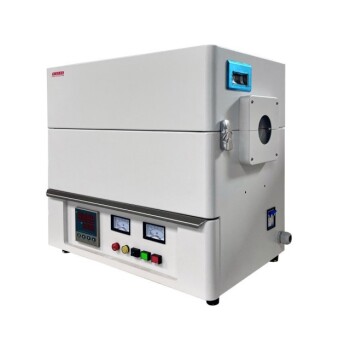
- Vacuum Sealed Continuous Working Rotary Tube Furnace Rotating Tube Furnace
- 1400℃ High Temperature Laboratory Tube Furnace with Alumina Tube
- 1700℃ High Temperature Laboratory Tube Furnace with Alumina Tube
- Magnesium Extraction and Purification Condensing Tube Furnace
- High Pressure Laboratory Vacuum Tube Furnace Quartz Tubular Furnace
People Also Ask
- What are some applications of rotary tube furnaces? Ideal for Continuous High-Temperature Material Processing
- What is the temperature range of some rotary tube furnaces? Achieve Uniform Heating Up to 1200°C
- What optional features enhance the processing capabilities of rotary tube furnaces? Boost Efficiency with Advanced Customizations
- When are rotary tube furnaces not suitable for a process? Avoid Costly Mistakes in Thermal Processing
- What are the advantages of rotary tube furnaces in fuel compatibility? Boost Efficiency and Cut Costs