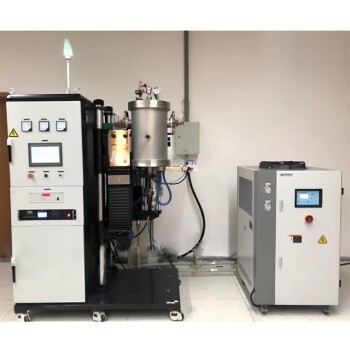
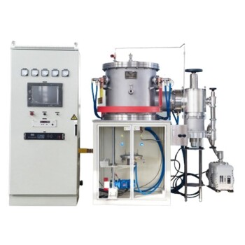
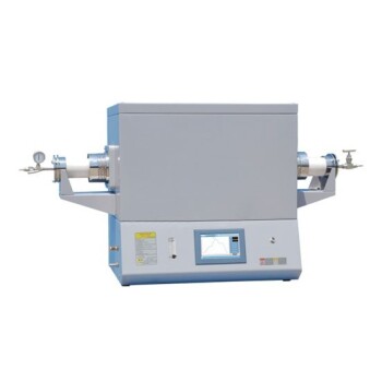
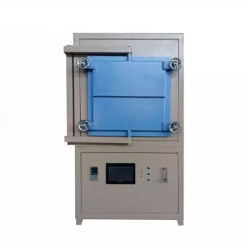
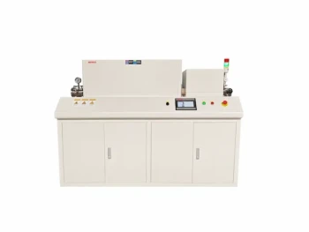
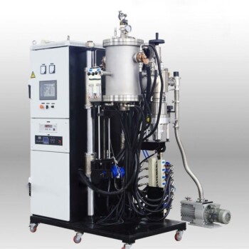
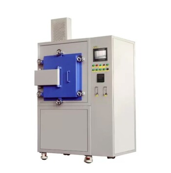
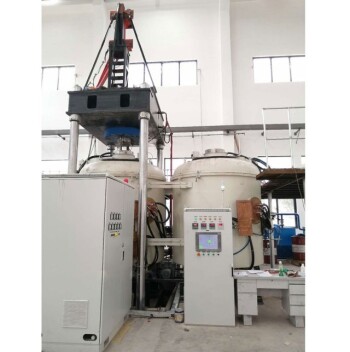
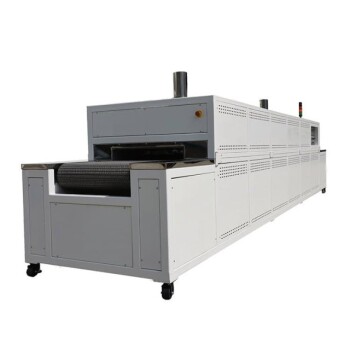
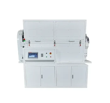
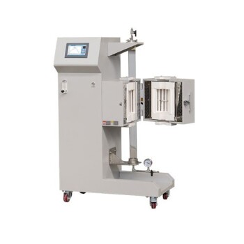
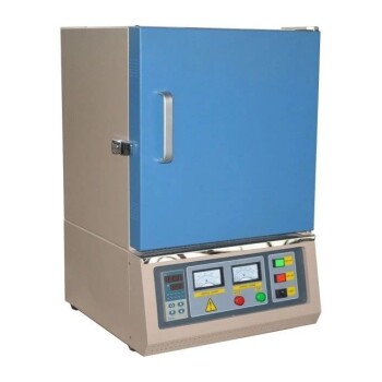
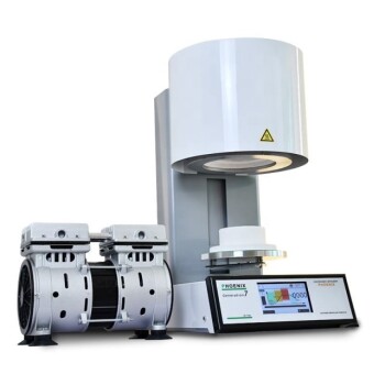
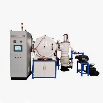
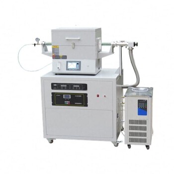
Annealing furnaces are the critical stabilization tools in the manufacturing of Indium Zinc Oxide (IZO) Thin Film Transistors (TFTs). They function as a post-deposition treatment system, typically heating the device to approximately 400°C in a controlled atmosphere to transform a raw, sputtered film into a functional, high-performance semiconductor.
Core Insight: Sputtering creates a film, but annealing creates a semiconductor. The heat treatment is essential to repair atomic-level damage caused during deposition, tuning the material so it can conduct electricity efficiently when turned "on" and insulate effectively when turned "off."
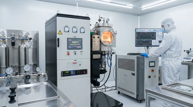
Transforming the Material Structure
The primary role of the annealing furnace is to correct the physical imperfections introduced during the initial manufacturing steps.
Repairing Structural Defects
Deposition methods like magnetron sputtering are physically energetic. They bombard the substrate with atoms, often resulting in a disordered atomic structure.
The thermal energy provided by the furnace allows atoms to migrate and settle into more stable positions. This "healing" process repairs structural defects that would otherwise impede electron flow.
Eliminating Internal Stress
As thin films are deposited, they often accumulate significant internal mechanical stress. If left untreated, this stress can lead to cracking, delamination, or inconsistent performance.
Annealing relaxes the material, releasing this built-up tension. This ensures the mechanical integrity of the thin film stack, which is vital for the long-term durability of the display or device.
Optimizing Electrical Performance
Beyond physical structure, the furnace directly dictates the electrical characteristics of the TFT.
Tuning Carrier Concentration
For a transistor to work, it must act as a switch—conductive at times, resistive at others.
The annealing atmosphere (often air) interacts with the IZO film to optimize the concentration of charge carriers. This process ensures the material does not behave like a conductive metal or a complete insulator, but rather a controllable semiconductor.
Enhancing Mobility and Stability
Mobility refers to how easily electrons move through the material. By removing defects that act as "roadblocks" for electrons, annealing significantly increases mobility.
This directly correlates to the On/Off ratio. A properly annealed device will have a high current when on and negligible leakage when off, ensuring distinct switching states and electrical stability over time.
Understanding the Process Variables
While necessary, the annealing process involves strict parameters that must be balanced carefully.
Temperature Precision
The reference temperature is generally around 400°C. This specific thermal budget is high enough to activate the material but must be controlled to avoid damaging the substrate or other device layers.
Atmospheric Control
The specific gas environment (such as air or oxygen-rich atmospheres) is as important as the heat.
The atmosphere dictates the chemical reaction at the surface of the film. An incorrect atmosphere can lead to an excess or deficiency of oxygen vacancies, which would ruin the semiconductor properties of the IZO layer.
Making the Right Choice for Your Goal
When configuring your annealing process for IZO TFTs, consider your specific performance targets.
- If your primary focus is Electrical Efficiency: Prioritize temperature stability to maximize electron mobility, ensuring the fastest possible switching speeds.
- If your primary focus is Device Reliability: Focus on the duration of the cycle to ensure complete relaxation of internal stresses, reducing the risk of physical failure.
Ultimately, the annealing furnace is the gatekeeper of quality, determining whether a deposited film becomes a high-performance electronic component.
Summary Table:
| Key Function | Impact on IZO TFTs |
|---|---|
| Repairs Structural Defects | Heals atomic-level damage from sputtering, enabling efficient electron flow. |
| Relieves Internal Stress | Prevents cracking/delamination, ensuring mechanical integrity and device longevity. |
| Optimizes Electrical Properties | Tunes carrier concentration for a high on/off ratio and enhances electron mobility. |
| Ensures Process Control | Precise temperature (~400°C) and atmosphere control are critical for consistent results. |
Ready to achieve superior performance and reliability for your IZO TFTs?
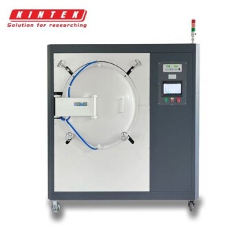
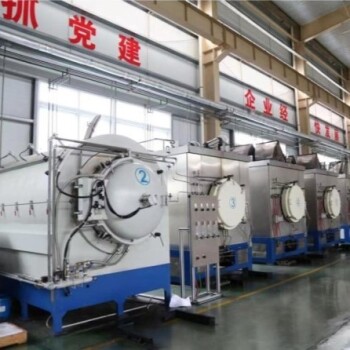
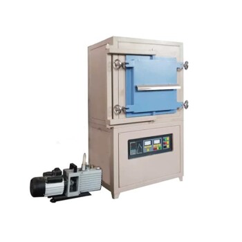
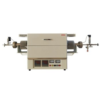
The precise thermal processing described is critical to your success. KINTEK's advanced annealing furnaces provide the exact temperature stability and atmospheric control required to transform your thin films into high-performance, durable semiconductors.
Backed by expert R&D and manufacturing, KINTEK offers Muffle, Tube, Rotary, Vacuum, and CVD systems, all customizable for your unique research and production needs.
Contact our experts today to discuss how a KINTEK furnace can be tailored to optimize your annealing process and elevate your device quality.
Visual Guide

Related Products
- Vacuum Heat Treat Sintering Furnace Molybdenum Wire Vacuum Sintering Furnace
- 2200 ℃ Tungsten Vacuum Heat Treat and Sintering Furnace
- 1700℃ High Temperature Laboratory Tube Furnace with Alumina Tube
- 1400℃ Controlled Inert Nitrogen Atmosphere Furnace
- Vacuum Heat Treat Furnace with Ceramic Fiber Liner
People Also Ask
- Why are synthesized CdS nanorods dried in a laboratory vacuum oven? Preserving Nanostructure and Chemical Integrity
- Why is high-purity argon protection required during the casting of alloy steel samples? Preserve Sample Integrity
- What is the core function of high-strength fan blades in a vacuum tempering furnace? Ensure Thermal Uniformity.
- How does a laboratory furnace address the strength-ductility trade-off in UFG titanium? Master Thermal Processing.
- What functions does glucose perform in lithium-ion sieve synthesis? Enhance Carbothermal Reduction for LiMnO2 Purity
