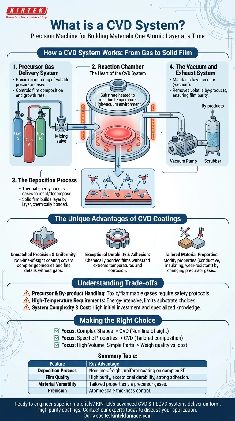
At its core, a Chemical Vapor Deposition (CVD) system is a precision machine for building materials one atomic layer at a time. It functions by introducing volatile precursor gases into a reaction chamber, where they decompose and react on a heated surface (the substrate) to form an exceptionally thin and uniform solid film. The system's main components—a gas delivery system, a heated reaction chamber, and a vacuum system—work in concert to create a highly controlled environment for this transformation from gas to solid.
A CVD system is not merely for applying a coating; it is a tool for fundamentally engineering a material's surface. Its true value lies in its ability to create durable, high-purity films with tailored properties on even the most complex three-dimensional objects, a feat impossible with conventional coating methods.
How a CVD System Works: From Gas to Solid Film
The entire CVD process is a carefully orchestrated sequence designed to control chemical reactions on a substrate's surface. Each component of the system plays a critical role in achieving the desired outcome.
The Precursor Gas Delivery System
This is the starting point of the process. The gas delivery system stores and precisely meters one or more volatile precursor gases. These gases contain the chemical elements required to build the final film.
The system's control over the gas mixture and flow rate is critical, as this directly influences the composition and growth rate of the final coating.
The Reaction Chamber
The reaction chamber is the heart of the CVD system. It is a sealed vessel, often a high-temperature vacuum furnace, that houses the substrate.
Inside the chamber, a heating mechanism raises the substrate's temperature to a specific point required to trigger the chemical reaction. Simultaneously, a vacuum system removes air and maintains a precise, low-pressure environment.
The Deposition Process
Once the substrate is heated and the chamber is at the correct pressure, the precursor gases are introduced. The thermal energy from the hot substrate causes the gases to react and/or decompose directly on its surface.
As the precursors break down, they deposit a solid film that is chemically bonded to the substrate. This process builds the film layer by layer, ensuring exceptional purity and structural integrity.
The Vacuum and Exhaust System
This system performs two essential functions. First, it maintains the low-pressure (vacuum) environment needed for the reaction. Second, it removes any volatile by-products created during the deposition process.
By continuously removing these unwanted gases, the system ensures the purity of the growing film and allows the deposition process to proceed efficiently.
The Unique Advantages of CVD Coatings
The reason CVD is so widely used in fields like microelectronics and advanced materials is that the films it produces have characteristics that are difficult or impossible to achieve otherwise.
Unmatched Precision and Uniformity
CVD offers exceptional control over a film's thickness, often with precision down to the atomic scale.
Because the deposition occurs from a gas phase, the coating is non-line-of-sight. This means it can uniformly cover every surface, including complex internal geometries and fine details, without the thin spots or gaps left by spray-on or sputtering methods.
Exceptional Durability and Adhesion
CVD films are not just layered on top of the substrate; they are chemically bonded to it. This creates an exceptionally strong and durable coating that can withstand extreme temperatures, thermal cycling, and corrosive environments.
Tailored Material Properties
The true power of CVD is its versatility. By changing the precursor gases, operators can precisely tailor the properties of the resulting film.
For example, using silane and ammonia gases can create a hard, insulating silicon nitride film. Switching to silane and nitrous oxide produces a silicon dioxide film, a fundamental component in electronics. This allows for the creation of films that are conductive, insulating, wear-resistant, or chemically inert.
Understanding the Trade-offs
While powerful, CVD technology involves complexities and limitations that must be considered. Objectivity requires acknowledging these challenges.
Precursor and By-product Handling
The precursor gases used in CVD are often toxic, flammable, or corrosive. The chemical by-products can also be hazardous. This necessitates sophisticated safety protocols and handling infrastructure, which adds to the operational cost and complexity.
High-Temperature Requirements
Many CVD processes require very high temperatures to initiate the desired chemical reactions. This consumes a significant amount of energy and limits the types of substrate materials that can be used, as some may not withstand the thermal stress.
System Complexity and Cost
The need for high-purity gas handling, vacuum technology, and precise temperature control makes CVD systems mechanically complex. Consequently, they have a high initial investment cost and require specialized knowledge for operation and maintenance.
Making the Right Choice for Your Goal
Deciding to use CVD depends entirely on the technical requirements of your application.
- If your primary focus is creating highly uniform, flawless coatings on complex shapes: CVD is an unparalleled choice due to its non-line-of-sight deposition process.
- If your primary focus is developing materials with specific electronic or mechanical properties: The ability to precisely control film composition makes CVD an essential research and manufacturing tool.
- If your primary focus is high-volume, low-cost surface treatment for simple parts: You must weigh the superior quality of CVD against the system's operational complexity and cost compared to simpler methods like painting or electroplating.
Ultimately, a CVD system provides atomic-level control over material creation, transforming simple surfaces into high-performance components.
Summary Table:
| Feature | Key Advantage |
|---|---|
| Deposition Process | Non-line-of-sight, uniform coating on complex 3D geometries |
| Film Quality | High purity, exceptional durability, and strong chemical adhesion |
| Material Versatility | Tailored properties (conductive, insulating, wear-resistant) via precursor gases |
| Precision | Atomic-scale thickness control for flawless film creation |
Ready to engineer superior materials with atomic-level precision?
KINTEK's advanced CVD and PECVD systems are engineered to meet your most demanding research and production needs. Leveraging our exceptional in-house R&D and manufacturing capabilities, we provide robust solutions—from standard models to deeply customized systems—that deliver the uniform, high-purity coatings critical for success in microelectronics and advanced materials.
Contact our experts today to discuss how a KINTEK CVD system can transform your application.
Visual Guide
Related Products
- HFCVD Machine System Equipment for Drawing Die Nano Diamond Coating
- Cylindrical Resonator MPCVD Machine System for Lab Diamond Growth
- Custom Made Versatile CVD Tube Furnace Chemical Vapor Deposition CVD Equipment Machine
- 915MHz MPCVD Diamond Machine Microwave Plasma Chemical Vapor Deposition System Reactor
- RF PECVD System Radio Frequency Plasma Enhanced Chemical Vapor Deposition
People Also Ask
- What is the function of high-purity Argon (Ar) gas during CVD? Optimize Your Thin Film Uniformity and Purity
- What materials are commonly used in CVD coating systems? Explore Key Materials for Superior Coatings
- What role does Chemical Vapor Deposition (CVD) equipment play in the surface coating of carbon fibers for composites?
- What core function does CVD equipment serve in h-BN anti-corrosion? Master Precision Synthesis for High-Performance Films
- What is Hot-filament Chemical Vapor Deposition (HFCVD)? Achieve High-Quality Thin Films with Precision Control