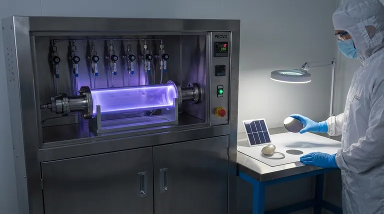
At its core, Plasma-Enhanced Chemical Vapor Deposition (PECVD) is a foundational process for creating high-performance thin films across numerous advanced industries. It is most commonly used for depositing insulating and protective layers in the fabrication of semiconductors, creating efficiency-boosting coatings for solar cells and LEDs, and applying protective barriers on materials ranging from medical implants to food packaging.
The defining advantage of PECVD is its ability to use an energy-rich plasma to deposit high-quality films at significantly lower temperatures than traditional methods. This unlocks the ability to coat temperature-sensitive materials that would otherwise be damaged or destroyed by conventional high-heat processes.
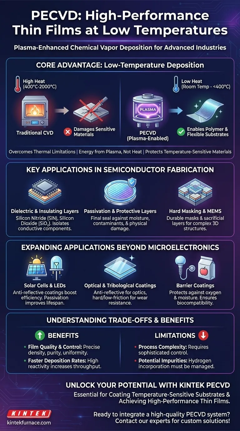
The Core Advantage: Low-Temperature Deposition
The primary reason PECVD is so widely adopted is its unique solution to the problem of heat. It fundamentally changes the energy requirements for film deposition.
Overcoming Thermal Limitations
Traditional Chemical Vapor Deposition (CVD) relies on very high temperatures, often between 400°C and 2000°C, to provide the energy needed for chemical reactions to occur on a substrate's surface.
This extreme heat makes conventional CVD incompatible with many materials, including polymers, flexible electronics, and certain complex semiconductor devices with pre-existing layers.
The Role of Plasma
PECVD circumvents this limitation by introducing energy in a different form: a plasma.
By applying an electric field to a gas, PECVD creates a plasma—an ionized state of matter containing highly reactive species. This plasma provides the activation energy for the chemical reactions, allowing for the deposition of a dense, high-quality film without requiring intense heat.
Enabling New Substrates
This low-temperature capability, sometimes operating down to room temperature, means PECVD can be used on a vast range of temperature-sensitive substrates. This has been a critical enabler for innovations in printable electronics, medical devices, and advanced optics.
Key Applications in Semiconductor Fabrication
PECVD is an indispensable workhorse in the semiconductor industry, essential for building the microscopic structures of integrated circuits and other micro-devices.
Dielectric and Insulating Layers
The most common application is depositing dielectric films, such as silicon nitride (SiN) and silicon dioxide (SiO₂). These films act as electrical insulators, isolating the millions of conductive components from each other on a single chip.
Passivation and Protective Layers
PECVD is used to apply a final protective layer, or passivation layer, to finished silicon wafers. This film seals the device, shielding it from moisture, contaminants, and physical damage that could cause it to fail.
Hard Masking and MEMS
In microelectromechanical systems (MEMS) and complex circuit patterning, PECVD films serve as durable hard masks or sacrificial layers. These temporary structures guide the etching process or help build up complex 3D geometries before being removed.
Expanding Applications Beyond Microelectronics
The versatility of PECVD has led to its adoption in a wide variety of other high-technology fields.
Solar Cells and LEDs
In photovoltaics, PECVD is used to deposit anti-reflective coatings that increase the amount of light absorbed by the solar cell. It also provides crucial passivation layers that improve the cell's overall electrical efficiency and lifespan. Similar principles apply to manufacturing high-brightness LEDs.
Optical and Tribological Coatings
PECVD is used to apply specialized coatings on glass and other surfaces. This includes creating anti-reflective layers for sunglasses and precision optical instruments or depositing extremely hard, low-friction films for components that require high wear resistance.
Barrier Coatings
The dense, uniform films created by PECVD form excellent barriers. This is used to protect flexible polymer substrates in electronics from oxygen and moisture, and even to apply an inert coating to the inside of food packaging like potato chip bags to preserve freshness. It is also used to coat medical implants to ensure biocompatibility.
Understanding the Trade-offs and Benefits
While powerful, choosing PECVD involves understanding its specific advantages and potential challenges compared to other methods.
Benefit: Film Quality and Control
PECVD allows for precise control over film properties like density, purity, and uniformity. The plasma-driven reactions can produce high-quality, conformal coatings that evenly cover even complex surface topographies.
Benefit: Faster Deposition Rates
The highly reactive nature of the plasma often leads to faster reaction kinetics and therefore higher deposition rates compared to some other low-temperature deposition techniques, improving manufacturing throughput.
Limitation: Process Complexity
A PECVD system is more complex than a simple thermal CVD reactor. Managing the plasma, gas flow, pressure, and RF power requires sophisticated control to ensure consistent and repeatable results.
Limitation: Potential Impurities
Because the process uses precursor gases that often contain hydrogen (e.g., silane), it is possible for hydrogen atoms to be incorporated into the deposited film. While this can sometimes be beneficial, it can also be an undesirable impurity that must be carefully managed.
Making the Right Choice for Your Goal
Selecting PECVD depends entirely on your material constraints and performance requirements.
- If your primary focus is fabricating integrated circuits or MEMS: PECVD is the industry standard for depositing high-quality dielectric, passivation, and structural layers without damaging thermally sensitive device architectures.
- If your primary focus is coating temperature-sensitive materials like polymers: PECVD is often the only viable choice, as its low-temperature process avoids substrate damage while still producing a dense, protective film.
- If your primary focus is enhancing optical or energy device performance: Use PECVD to engineer anti-reflective and passivation layers that directly boost the efficiency and durability of solar cells, LEDs, and optical components.
Ultimately, PECVD's ability to decouple the deposition process from high heat makes it one of the most versatile and essential tools in modern materials engineering.
Summary Table:
| Key Application Area | Primary Use of PECVD | Key Materials/Examples |
|---|---|---|
| Semiconductor Fabrication | Depositing dielectric insulating layers and protective passivation films. | Silicon Nitride (SiN), Silicon Dioxide (SiO₂) |
| Solar Cells & LEDs | Applying anti-reflective coatings and passivation layers to boost efficiency. | Photovoltaics, High-Brightness LEDs |
| Barrier & Protective Coatings | Creating dense, uniform barriers against moisture and oxygen on sensitive materials. | Medical Implants, Food Packaging, Flexible Electronics |
| Optical & Tribological Coatings | Depositing hard, wear-resistant or anti-reflective films on surfaces. | Precision Optics, Sunglasses, Mechanical Components |
Unlock the Potential of PECVD for Your Advanced Applications
PECVD's unique low-temperature capability is essential for coating temperature-sensitive substrates and achieving high-performance thin films. KINTEK leverages exceptional R&D and in-house manufacturing to provide advanced PECVD systems tailored to your specific needs.
Whether you are developing next-generation semiconductors, enhancing solar cell efficiency, or creating protective barriers for medical devices, our deep customization capabilities ensure your PECVD solution is precisely engineered for your unique experimental and production requirements.
Ready to integrate a high-quality, reliable PECVD system into your lab or production line? Contact our experts today to discuss how we can help you achieve superior thin film results.
Visual Guide
Related Products
- Slide PECVD Tube Furnace with Liquid Gasifier PECVD Machine
- RF PECVD System Radio Frequency Plasma Enhanced Chemical Vapor Deposition
- Inclined Rotary Plasma Enhanced Chemical Deposition PECVD Tube Furnace Machine
- Inclined Rotary Plasma Enhanced Chemical Deposition PECVD Tube Furnace Machine
- Multi Heating Zones CVD Tube Furnace Machine for Chemical Vapor Deposition Equipment
People Also Ask
- What are the advantages of using a tube furnace CVD system for Cu(111)/graphene? Superior Scalability and Quality
- How does a hydrogen reduction environment in an industrial tube furnace facilitate gold-copper alloy microspheres?
- What plasma source is used in PE-CVD tube furnaces? Unlock Low-Temperature, High-Quality Deposition
- What are the disadvantages of tube furnace cracking when processing heavy raw materials? Avoid Costly Downtime and Inefficiency
- What are the main advantages of PECVD tube furnaces compared to CVD tube furnaces? Lower Temp, Faster Deposition, and More


