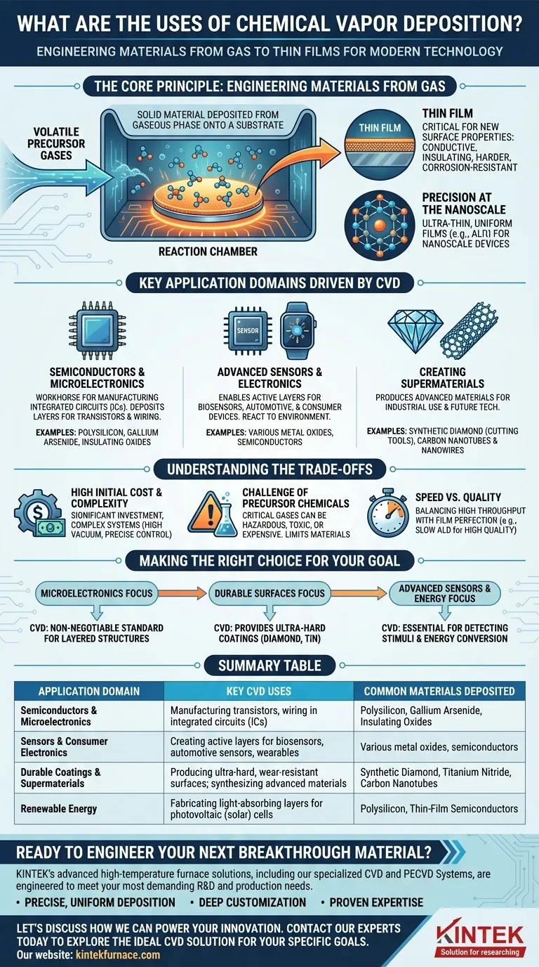
From the processor in your smartphone to advanced solar panels, Chemical Vapor Deposition (CVD) is a cornerstone manufacturing process used to create the high-performance, ultra-thin films that power modern technology. It is applied across a vast range of industries, including semiconductors, consumer electronics, automotive sensors, and renewable energy, to deposit critical materials like polysilicon, gallium arsenide, and even synthetic diamond films.
The true value of CVD is not merely in coating surfaces, but in its ability to construct entirely new materials, atom by atom. This precision allows engineers to design thin films with specific electrical, optical, or mechanical properties that are essential for high-performance devices.
The Core Principle: Engineering Materials from Gas
What is Chemical Vapor Deposition?
Chemical Vapor Deposition is a process where a solid material is deposited from a gaseous phase onto a substrate. Think of it as a highly controlled version of frost forming on a cold window pane.
In CVD, volatile precursor gases are introduced into a reaction chamber. When these gases come into contact with the heated substrate (the component being coated), they react or decompose, leaving a thin, solid film behind.
The Power of the Thin Film
The primary output of CVD is a thin film. These films are critical because they can grant a bulk material entirely new surface properties.
A thin film can make a surface electrically conductive, insulating, or semiconducting. It can make it harder, more corrosion-resistant, or change the way it interacts with light. This is the key to creating complex, layered devices like microchips.
Precision at the Nanoscale
Modern electronics demand incredible precision. CVD techniques, particularly Atomic Layer Deposition (ALD), allow for the deposition of films that are perfectly uniform and only a single atomic layer thick.
This level of control is fundamental to building the nanoscale transistors found in today's advanced processors and memory chips.
Key Application Domains Driven by CVD
Powering the Semiconductor Industry
CVD is the workhorse of microchip manufacturing. It is used to deposit the various layers that form the transistors and wiring within an Integrated Circuit (IC).
Materials like amorphous polysilicon and gallium arsenide, both deposited via CVD, are foundational for creating the logic gates and components in processors and photovoltaic cells.
Enabling Advanced Sensors and Electronics
The sensors in your car, smartphone, and smart home rely on specialized films to function. CVD is used to deposit the active layers in biosensors, HVAC sensors, and automotive electronics.
These films are engineered to react to specific changes in their environment, such as pressure, temperature, or the presence of a chemical. This capability also extends to consumer devices like hearables and wearables.
Creating Supermaterials
CVD is not limited to electronics. Specialized techniques like microwave plasma CVD can be used to grow some of the world's most advanced materials.
This includes producing films of polycrystalline and monocrystalline diamond, which are used for industrial cutting tools and wear-resistant coatings. It is also used to synthesize carbon nanotubes and nanowires, materials with extraordinary properties promising for future technologies.
Understanding the Trade-offs
High Initial Cost and Complexity
CVD systems are sophisticated and represent a significant capital investment. They often require high-vacuum environments, precise temperature controls, and complex gas handling systems, making the process expensive to set up and run.
The Challenge of Precursor Chemicals
The choice of precursor gases is critical to the quality of the final film. These chemicals can be hazardous, toxic, or expensive, requiring stringent safety protocols and handling procedures. The available chemistry can sometimes limit the types of materials that can be deposited.
Speed vs. Quality
There is often a direct trade-off between the speed of deposition and the quality of the resulting film. Processes like Atomic Layer Deposition produce exceptionally high-quality, uniform films, but they do so very slowly. For mass manufacturing, balancing throughput with film perfection is a constant engineering challenge.
Making the Right Choice for Your Goal
Ultimately, the use of CVD is dictated by the need for a material with properties that cannot be achieved otherwise.
- If your primary focus is microelectronics: CVD is the non-negotiable standard for creating the layered semiconducting and insulating structures in modern ICs.
- If your primary focus is creating durable surfaces: CVD provides ultra-hard coatings like synthetic diamond or titanium nitride for high-performance tools and wear-resistant components.
- If your primary focus is advanced sensors or energy: CVD is essential for depositing the active thin films that detect specific stimuli or convert light into electricity in solar cells.
Understanding CVD is to understand how we build the foundational materials of modern technology from the ground up.
Summary Table:
| Application Domain | Key CVD Uses | Common Materials Deposited |
|---|---|---|
| Semiconductors & Microelectronics | Manufacturing transistors, wiring in integrated circuits (ICs) | Polysilicon, Gallium Arsenide, Insulating Oxides |
| Sensors & Consumer Electronics | Creating active layers for biosensors, automotive sensors, wearables | Various metal oxides, semiconductors |
| Durable Coatings & Supermaterials | Producing ultra-hard, wear-resistant surfaces; synthesizing advanced materials | Synthetic Diamond, Titanium Nitride, Carbon Nanotubes |
| Renewable Energy | Fabricating light-absorbing layers for photovoltaic (solar) cells | Polysilicon, Thin-Film Semiconductors |
Ready to Engineer Your Next Breakthrough Material?
Chemical Vapor Deposition is the key to creating the high-performance thin films that define modern technology. Whether you are developing advanced semiconductors, sensitive sensors, or ultra-durable coatings, the right CVD solution is critical.
KINTEK's advanced high-temperature furnace solutions, including our specialized CVD and PECVD Systems, are engineered to meet your most demanding R&D and production needs. Leveraging our exceptional in-house R&D and manufacturing capabilities, we provide:
- Precise, Uniform Deposition: Achieve the consistent, high-quality thin films your applications require.
- Deep Customization: We tailor our systems to your unique process parameters and material challenges.
- Proven Expertise: From R&D labs to pilot production, we help you scale your technology from concept to reality.
Let's discuss how we can power your innovation. Contact our experts today to explore the ideal CVD solution for your specific goals.
Visual Guide
Related Products
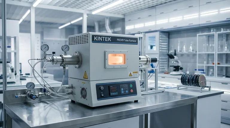
- Custom Made Versatile CVD Tube Furnace Chemical Vapor Deposition CVD Equipment Machine
- MPCVD Machine System Reactor Bell-jar Resonator for Lab and Diamond Growth
- Multi Heating Zones CVD Tube Furnace Machine for Chemical Vapor Deposition Equipment
- 915MHz MPCVD Diamond Machine Microwave Plasma Chemical Vapor Deposition System Reactor
- Slide PECVD Tube Furnace with Liquid Gasifier PECVD Machine
People Also Ask
- Why are CVD tube furnace sintering systems indispensable for 2D material research and production? Unlock Atomic-Scale Precision
- What future trends are expected in the development of CVD tube furnaces? Discover Smarter, More Versatile Systems
- What temperature range do standard CVD tube furnaces operate at? Unlock Precision for Your Material Deposition
- How can integrating CVD tube furnaces with other technologies benefit device fabrication? Unlock Advanced Hybrid Processes
- What are the practical applications of gate media prepared by CVD tube furnaces? Unlock Advanced Electronics and More


