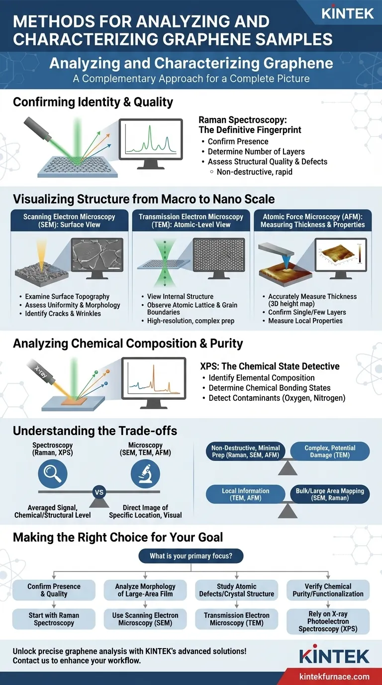
To analyze and characterize graphene samples, researchers rely on a suite of microscopic and spectroscopic techniques. The most common methods are Raman spectroscopy, electron microscopy (both Scanning and Transmission), and X-ray Photoelectron Spectroscopy (XPS), each providing a unique piece of information about the material's identity, structure, and purity.
Graphene characterization is not about finding a single "best" method. It requires a complementary approach, where each technique provides a unique piece of the puzzle—from confirming its fundamental identity and quality to visualizing its structure and chemical purity.
Confirming Graphene's Identity and Quality
The first step in any analysis is confirming that you actually have graphene and assessing its fundamental quality. For this, spectroscopy is the primary tool.
Raman Spectroscopy: The Definitive Fingerprint
Raman spectroscopy is the most important, rapid, and non-destructive technique for identifying graphene. By shining a laser on the sample and analyzing the scattered light, it provides a unique spectral "fingerprint."
This fingerprint can definitively confirm the presence of graphene, determine the number of layers (distinguishing single-layer from bilayer or multilayer), and assess the material's structural quality and defect density.
Visualizing Structure from Macro to Nano Scale
After confirming its identity, you need to see the material. Microscopy techniques allow you to visualize the graphene's physical form, from the overall film down to its individual atoms.
Scanning Electron Microscopy (SEM): The Surface View
SEM is used to examine the surface topography and morphology of a sample over relatively large areas.
It is excellent for assessing the uniformity of a graphene film, identifying cracks or wrinkles, and determining the size and distribution of graphene flakes in a composite material.
Transmission Electron Microscopy (TEM): The Atomic-Level View
TEM provides extremely high-resolution images by passing an electron beam through an ultra-thin sample.
This technique is essential for viewing the internal structure of the material, including the atomic lattice, dislocations, grain boundaries, and the precise stacking of layers.
Atomic Force Microscopy (AFM): Measuring Thickness and Properties
AFM uses a physical probe to scan the sample's surface, creating a 3D height map with nanoscale precision.
Its primary use for graphene is to accurately measure the thickness of a flake, which directly confirms if it is a single, double, or few-layer sheet. It can also be used to measure local properties like friction or conductivity.
Analyzing Chemical Composition and Purity
Graphene is often modified or can become contaminated during production. Chemical analysis is critical for applications where purity is paramount.
X-ray Photoelectron Spectroscopy (XPS): The Chemical State Detective
XPS is a surface-sensitive technique that identifies the elemental composition and, crucially, the chemical bonding states of those elements.
For graphene, XPS is used to detect the presence of oxygen (in graphene oxide), nitrogen (in doped graphene), or any other elemental contaminants. It tells you not just what is there, but how it's bonded to the carbon lattice.
Understanding the Trade-offs
No single technique tells the whole story. Understanding their limitations is key to designing a proper characterization workflow.
Spectroscopy vs. Microscopy
Spectroscopy methods like Raman and XPS typically provide an averaged signal over the area illuminated by the laser or X-ray beam. They answer "what is this?" on a chemical and structural level.
Microscopy (SEM, TEM, AFM) gives you a direct image of a specific location. It answers "what does this look like?" at a specific point, but it doesn't give chemical information on its own.
Sample Preparation and Destructiveness
Methods like Raman, SEM, and AFM are generally non-destructive and require minimal sample preparation.
In contrast, TEM requires complex and difficult sample preparation, which involves transferring the graphene to a special grid and can potentially damage the sample.
Local vs. Bulk Information
TEM and AFM provide highly localized information about a tiny portion of your sample. SEM and Raman can be used to map larger areas, giving a better picture of the sample's overall uniformity.
Making the Right Choice for Your Goal
Your characterization strategy should be driven by the specific question you need to answer.
- If your primary focus is confirming the presence and quality of graphene: Start with Raman Spectroscopy as it is the fastest and most definitive method for identifying layers and defects.
- If your primary focus is analyzing the morphology of a large-area film: Use Scanning Electron Microscopy (SEM) to check for coverage, uniformity, and large-scale defects.
- If your primary focus is studying atomic-level defects or crystal structure: Transmission Electron Microscopy (TEM) is essential, despite its complex sample preparation.
- If your primary focus is verifying chemical purity or analyzing functionalization: Rely on X-ray Photoelectron Spectroscopy (XPS) to detect contaminants and determine bonding states.
Ultimately, a multi-technique approach is the only way to build a complete and accurate picture of your graphene material.
Summary Table:
| Technique | Primary Use | Key Insights |
|---|---|---|
| Raman Spectroscopy | Confirm identity and quality | Detects layers, defects, and structural quality |
| Scanning Electron Microscopy (SEM) | Visualize surface morphology | Assesses uniformity, cracks, and flake distribution |
| Transmission Electron Microscopy (TEM) | Examine atomic-level structure | Views lattice, grain boundaries, and layer stacking |
| X-ray Photoelectron Spectroscopy (XPS) | Analyze chemical composition | Identifies elements, bonding states, and contaminants |
| Atomic Force Microscopy (AFM) | Measure thickness and properties | Provides 3D height maps and local property data |
Unlock precise graphene analysis with KINTEK's advanced solutions! Leveraging exceptional R&D and in-house manufacturing, we provide diverse laboratories with high-temperature furnaces like Muffle, Tube, Rotary, Vacuum & Atmosphere Furnaces, and CVD/PECVD Systems. Our strong deep customization capability ensures your unique experimental needs are met. Contact us today to enhance your material characterization workflow!
Visual Guide