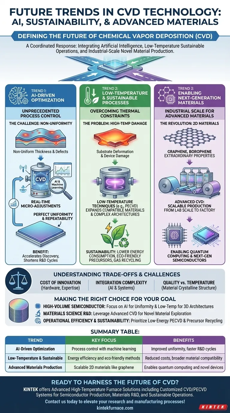
The future of Chemical Vapor Deposition (CVD) is being defined by three primary forces: the integration of artificial intelligence for process control, the urgent push for lower-temperature and sustainable operation, and the drive to manufacture novel, advanced materials at industrial scale. These trends are not isolated improvements but a coordinated response to the increasing demands of next-generation electronics, quantum computing, and sustainable manufacturing.
At its core, the evolution of CVD is no longer just about depositing known materials better. It's about overcoming fundamental limitations in temperature, cost, and environmental impact to enable the creation of next-generation devices and structures that are currently impossible to produce at scale.
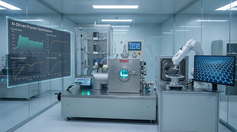
Trend 1: AI-Driven Optimization for Unprecedented Control
The Problem of Non-Uniformity
A classic challenge in CVD is achieving perfectly uniform film thickness and properties, especially over the large substrates used in modern semiconductor and display manufacturing. Minor fluctuations in temperature, pressure, or gas flow can lead to defects and inconsistent device performance.
AI as the Process Guardian
The future of process control is AI-driven optimization. By integrating machine learning algorithms with real-time sensor data, CVD systems can make continuous, micro-adjustments to process parameters. This ensures unparalleled uniformity and repeatability, directly addressing the challenge of large-area deposition.
Beyond Control: Accelerating Discovery
This intelligent control extends beyond maintaining consistency. AI can also be used to rapidly explore and optimize deposition conditions for entirely new materials, drastically shortening the research and development cycle.
Trend 2: The Push for Low-Temperature and Sustainable Processes
Overcoming Thermal Constraints
Traditional thermal CVD requires extremely high temperatures. This heat can deform or even destroy delicate substrates, such as polymers, or damage previously fabricated layers in a complex semiconductor device.
The Rise of Low-Temperature CVD
A major development direction is the refinement of low-temperature techniques, such as Plasma-Enhanced CVD (PECVD). These methods allow for high-quality film deposition at significantly lower temperatures, expanding the range of compatible materials and enabling more complex, multi-layered device architectures.
Reducing Environmental and Energy Footprints
This trend has a critical dual benefit: sustainability. Lower-temperature processes inherently consume less energy, reducing operational costs and carbon footprint. Furthermore, active research is focused on developing eco-friendly precursor chemistries and gas recycling systems to minimize toxic by-products and waste.
Trend 3: Enabling the Next Generation of Materials
The 2D Materials Revolution
CVD is becoming the key technology for producing revolutionary 2D materials, such as graphene and borophene. These single-atom-thick layers possess extraordinary electronic and mechanical properties, making them essential for future technologies.
The Challenge of Scalability
The promise of 2D materials can only be realized if they can be manufactured reliably, without defects, and on an industrial scale. Advanced CVD techniques are being developed specifically to solve this problem, moving these materials from the laboratory to the factory.
Impact on Next-Gen Computing
The ability to produce high-quality, large-area 2D materials via CVD is a critical enabler for quantum computing and next-generation semiconductors. These applications demand a level of material perfection and scalability that only advanced deposition technologies can provide.
Understanding the Trade-offs and Challenges
The Cost of Innovation
Implementing AI control systems and developing new low-temperature processes requires significant upfront investment in both hardware and expertise. Similarly, novel precursor materials are often expensive, presenting a cost barrier to adoption.
Integration Complexity
AI-driven systems are not "plug-and-play." They require careful integration with existing hardware and specialized knowledge to maintain and fine-tune the control algorithms effectively.
Quality vs. Temperature
While low-temperature processes solve many problems, a key trade-off can be film quality. For some specific materials, the crystalline structure and density achieved at high temperatures may still be superior to what is possible with current low-temperature methods.
Making the Right Choice for Your Goal
To navigate these trends, it is crucial to align them with your specific objectives.
- If your primary focus is high-volume semiconductor manufacturing: The dual benefit of AI for large-wafer uniformity and low-temp processes for advanced 3D chip architectures are your most critical trends.
- If your primary focus is materials science and R&D: Your key takeaway is leveraging advanced CVD to explore and scale novel materials like 2D films, which were previously lab-scale curiosities.
- If your primary focus is operational efficiency and sustainability: The most important developments are low-energy PECVD and ongoing research into precursor recycling to reduce both costs and environmental impact.
Ultimately, the future of CVD lies in its transformation from a deposition tool into an intelligent, sustainable, and versatile advanced manufacturing platform.
Summary Table:
| Trend | Key Focus | Benefits |
|---|---|---|
| AI-Driven Optimization | Process control with machine learning | Improved uniformity, faster R&D cycles |
| Low-Temperature & Sustainable Processes | Energy efficiency and eco-friendly methods | Reduced costs, broader material compatibility |
| Advanced Materials Production | Scalable 2D materials like graphene | Enables quantum computing and novel devices |
Ready to harness the future of CVD for your lab? At KINTEK, we leverage exceptional R&D and in-house manufacturing to provide advanced high-temperature furnace solutions, including CVD/PECVD systems. Our strong deep customization capability ensures we precisely meet your unique experimental needs, whether for semiconductor production, materials R&D, or sustainable operations. Contact us today to discuss how our tailored solutions can elevate your research and manufacturing processes!
Visual Guide
Related Products
- Custom Made Versatile CVD Tube Furnace Chemical Vapor Deposition CVD Equipment Machine
- Multi Heating Zones CVD Tube Furnace Machine for Chemical Vapor Deposition Equipment
- HFCVD Machine System Equipment for Drawing Die Nano Diamond Coating
- Split Chamber CVD Tube Furnace with Vacuum Station CVD Machine
- 915MHz MPCVD Diamond Machine Microwave Plasma Chemical Vapor Deposition System Reactor
People Also Ask
- What is a CVD tube furnace and what is its primary function? Discover Precision Thin-Film Deposition
- What customization options are available for CVD tube furnaces? Tailor Your System for Superior Material Synthesis
- Which industries and research fields benefit from CVD tube furnace sintering systems for 2D materials? Unlock Next-Gen Tech Innovations
- What are the practical applications of gate media prepared by CVD tube furnaces? Unlock Advanced Electronics and More
- How might AI and machine learning enhance CVD tube furnace processes? Boost Quality, Speed, and Safety


