In modern engineering, Chemical Vapor Deposition (CVD) is the foundational process for creating the high-performance thin films that power our most advanced technologies. It is the key manufacturing method behind semiconductor chips, durable protective coatings, and a wide range of electronic sensors. Specific applications include depositing the microscopic layers in computer processors, creating wear-resistant diamond films, and fabricating sensitive components for automotive, consumer, and medical devices.
The true value of CVD isn't just the wide range of products it helps create, but how it creates them. By building materials atom-by-atom from a gas phase, CVD provides unparalleled control over a film's thickness, purity, and conformity to a surface, making it indispensable for manufacturing microscopic and high-performance components.
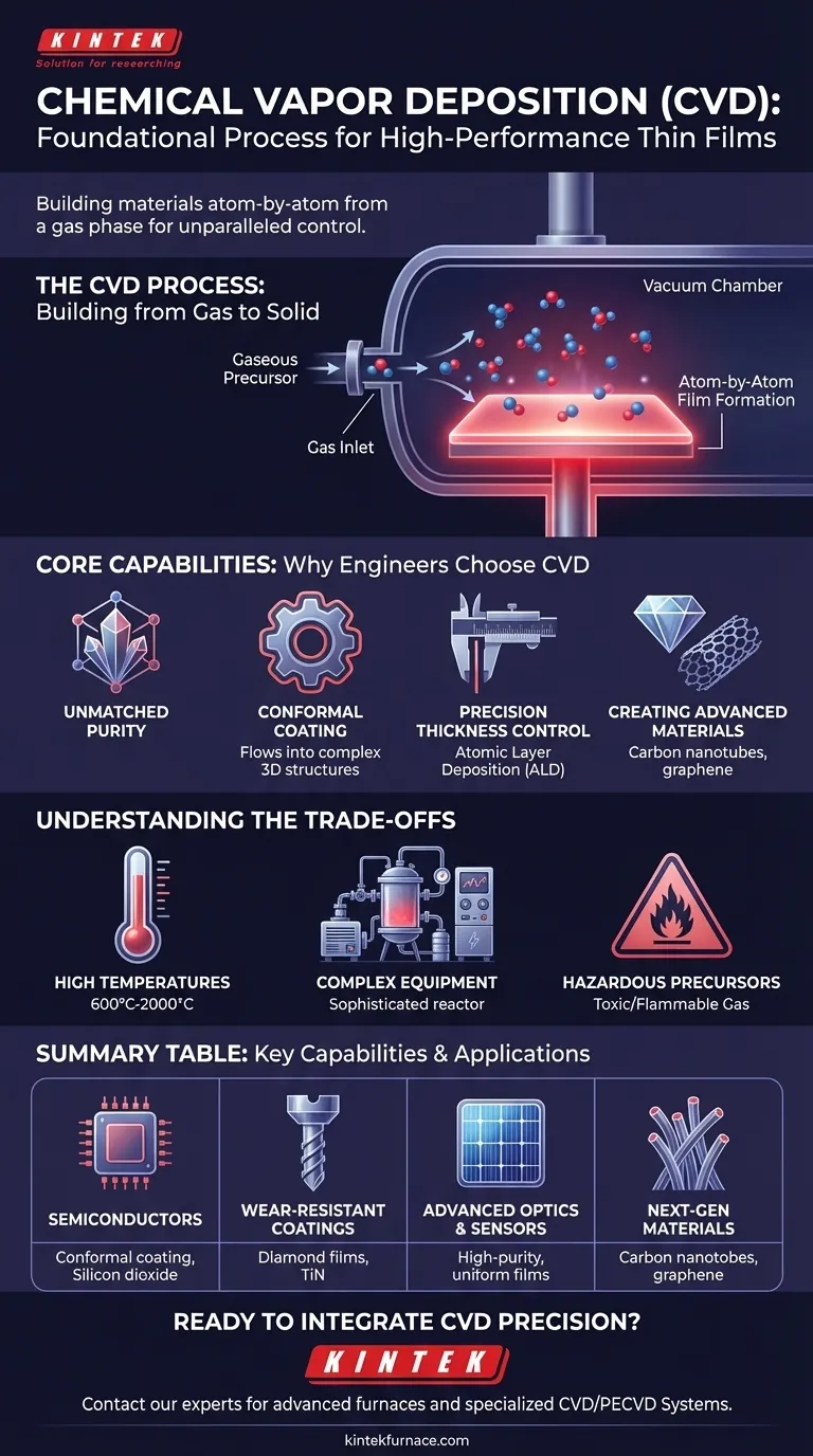
What Is Chemical Vapor Deposition?
CVD is a vacuum-based process where solid materials are grown on a substrate (a base material or wafer) through a series of controlled chemical reactions. It is less like painting a surface and more like building a crystal structure one layer at a time.
A Process of Building from Gas
The process begins by introducing precise amounts of gaseous precursor chemicals into a high-vacuum reaction chamber. This controlled environment is critical for preventing contamination from the outside atmosphere.
The Role of Heat and a Substrate
Inside the chamber, the substrate is heated to high temperatures. This heat provides the energy needed to trigger a chemical reaction or cause the precursor gases to decompose directly on the substrate's surface.
Atom-by-Atom Film Formation
As the gases react or decompose, they form a solid, stable thin film that bonds to the substrate. Because this happens molecule by molecule, the resulting layer is extremely uniform and high-quality, creating a durable dry coating without any need for post-process curing.
The Core Capabilities: Why Engineers Choose CVD
Engineers don't choose CVD because it is simple, but because it delivers capabilities that other methods cannot. Its power lies in its precision and versatility at a microscopic scale.
Unmatched Purity and Quality
Operating in a high-vacuum environment minimizes impurities and defects. This results in high-performance solid materials with predictable and reliable electrical, optical, or mechanical properties.
Conformal Coating for Complex Shapes
CVD is not a "line-of-sight" process. The precursor gas flows around and into even the most complex, microscopic three-dimensional structures. This results in a conformal film—a layer with a perfectly uniform thickness across the entire surface, including inside trenches and around sharp corners.
Precision Thickness Control
The process allows for exceptionally fine control over the final thickness of the deposited film. Specialized techniques like Atomic Layer Deposition (ALD), a subtype of CVD, can deposit a film that is literally one single layer of atoms at a time.
Creating Advanced Materials
CVD is one of the few commercially viable methods for creating exotic and high-performance materials. This includes synthesizing polycrystalline diamond films for wear resistance and thermal management, as well as growing carbon nanotubes and nanowires for next-generation electronics.
Understanding the Trade-offs
While powerful, CVD is not the right solution for every problem. Its precision comes with specific requirements and limitations that must be considered.
Requirement for High Temperatures
The chemical reactions in CVD often demand high temperatures, typically from 600°C to over 2000°C. This can limit the types of substrate materials that can be used, as some plastics or sensitive electronic components cannot withstand the heat.
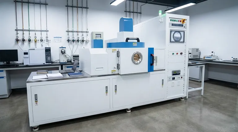
Complex and Expensive Equipment
CVD reactors are sophisticated systems. They require high-vacuum pumps, precise gas flow controllers, high-temperature heating elements, and automated control systems to function. This complexity leads to significant capital investment and maintenance costs.
Use of Precursor Chemicals
The precursor gases used in CVD can be toxic, flammable, or corrosive. This necessitates strict safety protocols, specialized handling equipment, and exhaust gas management systems, adding to the operational complexity.
Making the Right Choice for Your Goal
Selecting a deposition method depends entirely on the technical and economic requirements of your project. CVD excels where ultimate performance is the goal.
- If your primary focus is ultimate precision and thinness: CVD, particularly its variant Atomic Layer Deposition (ALD), is the industry standard for controlling film thickness at the atomic scale.
- If your primary focus is coating complex, three-dimensional microstructures: The uniquely conformal nature of CVD makes it far superior to line-of-sight methods for ensuring complete and uniform coverage.
- If your primary focus is creating highly durable or exotic materials: CVD is uniquely capable of synthesizing materials like synthetic diamond films or carbon nanotubes that are difficult or impossible to produce otherwise.
- If your primary focus is a simple, low-cost coating on a flat surface: You may want to explore less complex alternatives, as the equipment and operational costs of CVD are significant.
Ultimately, leveraging CVD is about choosing a process where atomic-level control over a material's structure is not just a benefit, but a fundamental requirement for success.
Summary Table:
| Application Area | Key CVD Capability | Common Materials/Examples |
|---|---|---|
| Semiconductors & Microelectronics | Conformal coating, atomic-level thickness control | Silicon dioxide, silicon nitride, tungsten layers on chips |
| Wear-Resistant & Protective Coatings | Synthesis of hard, durable materials | Diamond films, titanium nitride (TiN) coatings on tools |
| Advanced Optics & Sensors | High-purity, uniform films with precise properties | Thin-film solar cells, optical filters, gas sensors |
| Next-Generation Materials | Growth of nanostructures and exotic materials | Carbon nanotubes, graphene, nanowires |
Ready to Integrate CVD Precision into Your Lab?
Leveraging exceptional R&D and in-house manufacturing, KINTEK provides diverse laboratories with advanced high-temperature furnace solutions tailored for Chemical Vapor Deposition processes. Our product line—including Tube Furnaces, Vacuum & Atmosphere Furnaces, and specialized CVD/PECVD Systems—is complemented by our strong deep customization capability to precisely meet your unique experimental requirements, whether for R&D or production.
Let us help you achieve unparalleled control over your thin films. Contact our experts today to discuss your specific CVD application needs.
Visual Guide
Related Products
- Custom Made Versatile CVD Tube Furnace Chemical Vapor Deposition CVD Equipment Machine
- RF PECVD System Radio Frequency Plasma Enhanced Chemical Vapor Deposition
- MPCVD Machine System Reactor Bell-jar Resonator for Lab and Diamond Growth
- 915MHz MPCVD Diamond Machine Microwave Plasma Chemical Vapor Deposition System Reactor
- Slide PECVD Tube Furnace with Liquid Gasifier PECVD Machine
People Also Ask
- Why are CVD tube furnace sintering systems indispensable for 2D material research and production? Unlock Atomic-Scale Precision
- What is a CVD tube furnace and what is its primary function? Discover Precision Thin-Film Deposition
- What are the key features of CVD tube furnaces for 2D material processing? Unlock Precision Synthesis for Superior Materials
- How might AI and machine learning enhance CVD tube furnace processes? Boost Quality, Speed, and Safety
- How does CVD tube furnace sintering enhance graphene growth? Achieve Superior Crystallinity and High Electron Mobility


