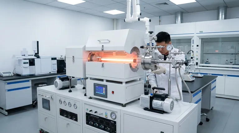
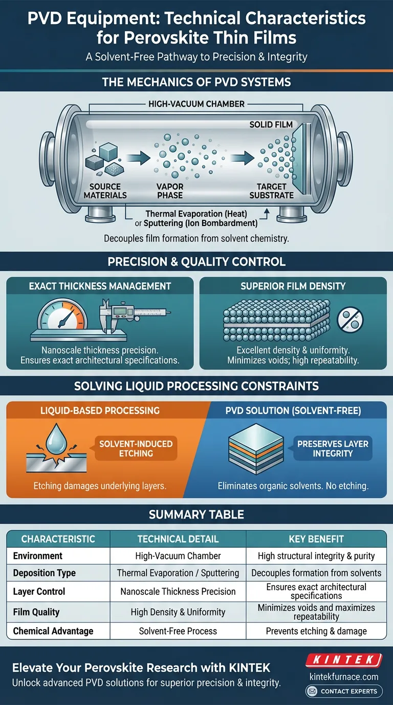
Physical Vapor Deposition (PVD) systems operate within high-vacuum environments to transform solid precursors into a gaseous phase before condensing them onto a substrate. Utilizing techniques such as thermal evaporation and sputtering, this equipment allows for the fabrication of perovskite thin films without the involvement of liquid solvents.
The core value of PVD equipment lies in its ability to decouple film formation from solvent chemistry. This grants researchers precise control over layer thickness and density while eliminating the solvent-induced damage often encountered in liquid-based processing.
The Mechanics of PVD Systems
High-Vacuum Phase Transformation
The fundamental characteristic of PVD equipment is the creation of a high-vacuum environment.
Within this controlled chamber, solid source materials are converted into a gas.
This vapor is then directed to re-condense onto the target substrate, forming a solid film.
Specific Deposition Techniques
PVD encompasses distinct mechanical approaches to achieving this phase change.
Thermal evaporation uses heat to vaporize the source material.
Sputtering utilizes ion bombardment to eject material from a target source into the vapor phase.
Precision and Quality Control
Exact Thickness Management
One of the distinct technical advantages of PVD is the ability to dictate the geometry of the film.
Operators can achieve precise control over the thickness of each individual thin-film layer.
This precision ensures that the final stack meets exact architectural specifications.
Superior Film Density and Repeatability
The nature of vacuum deposition results in films with high structural integrity.
PVD processes produce films characterized by excellent density, minimizing voids that can occur in other methods.
Furthermore, the process offers high repeatability, ensuring consistent results across multiple fabrication runs.
Solving Liquid Processing Constraints
The Solvent-Free Advantage
PVD equipment fundamentally changes the chemistry of fabrication by eliminating organic solvents.
This allows for the processing of materials that might otherwise be sensitive to chemical dissolution.
Preventing Solvent-Induced Etching
A critical issue in building multi-layer perovskite devices is the damage caused by solvents.
Liquid-based processing often leads to solvent-induced etching, where the application of a new layer dissolves or damages the one beneath it.
PVD avoids this problem entirely, preserving the integrity of underlying layers during the deposition of subsequent films.
Making the Right Choice for Your Goal
PVD equipment offers a distinct set of capabilities for researchers prioritizing structural control and chemical stability.
- If your primary focus is architectural precision: Leverage PVD for its ability to strictly control layer thickness and ensure high film density.
- If your primary focus is multi-layer integrity: Choose PVD to eliminate organic solvents and prevent the etching problems inherent in liquid-based processing.
By removing solvents from the equation, PVD provides a robust pathway to high-quality, reproducible perovskite films.
Summary Table:
| Characteristic | Technical Detail | Key Benefit |
|---|---|---|
| Environment | High-Vacuum Chamber | High structural integrity & purity |
| Deposition Type | Thermal Evaporation / Sputtering | Decouples film formation from solvent chemistry |
| Layer Control | Nanoscale Thickness Precision | Ensures exact architectural specifications |
| Film Quality | High Density & Uniformity | Minimizes voids and maximizes repeatability |
| Chemical Advantage | Solvent-Free Process | Prevents etching and damage to underlying layers |
Elevate Your Perovskite Research with KINTEK
Unlock superior architectural precision and multi-layer integrity with KINTEK’s advanced PVD solutions. Backed by expert R&D and world-class manufacturing, we provide high-performance Vacuum, CVD, and specialized thin-film systems tailored to your laboratory’s unique requirements. Whether you are scaling up solar cell production or conducting fundamental material science, our customizable high-temperature and vacuum equipment ensures repeatable, solvent-free results.
Ready to eliminate solvent-induced etching and achieve high-density films?
Visual Guide
References
- Azam Khorasani, Mojtaba Abdi‐Jalebi. Opportunities, Challenges, and Strategies for Scalable Deposition of Metal Halide Perovskite Solar Cells and Modules. DOI: 10.1002/aesr.202300275
This article is also based on technical information from Kintek Furnace Knowledge Base .
Related Products
- HFCVD Machine System Equipment for Drawing Die Nano Diamond Coating
- Slide PECVD Tube Furnace with Liquid Gasifier PECVD Machine
- MPCVD Machine System Reactor Bell-jar Resonator for Lab and Diamond Growth
- Custom Made Versatile CVD Tube Furnace Chemical Vapor Deposition CVD Equipment Machine
- RF PECVD System Radio Frequency Plasma Enhanced Chemical Vapor Deposition
People Also Ask
- What is the significance of the vacuum pressure control system in the CVD coating process for powders?
- What is the advantage of using a CVD system for coating turbine blades? Master Complex Geometries with Ease
- What is the function of high-purity Argon (Ar) gas during CVD? Optimize Your Thin Film Uniformity and Purity
- What are the equipment for chemical vapor deposition? A Guide to the 5 Essential Components
- How can customers maximize the quality of CVD coatings? Master Pre-Coating Prep for Superior Results


