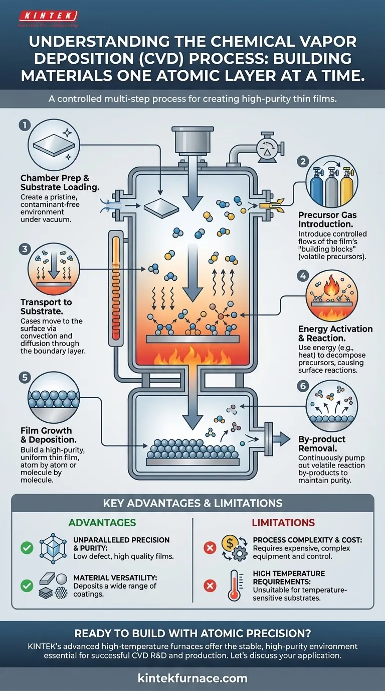
In essence, Chemical Vapor Deposition (CVD) is a multi-step process where precursor gases are introduced into a controlled chamber, energized (typically with heat), and chemically react to form a solid, high-purity thin film on a substrate. The core sequence involves transporting reactive gases, inducing chemical reactions on or near the substrate's surface, the subsequent deposition of the solid material, and the removal of gaseous by-products.
The true power of CVD lies not just in its steps, but in the precise control over each one. By manipulating gas flow, temperature, and pressure, you are essentially building a material from the ground up, one atomic or molecular layer at a time.
The Foundational Goal: Building with Atomic Precision
At its heart, CVD is a deposition method performed under controlled conditions, often a vacuum, to build thin films with exceptional quality. It is not like painting or dipping; it is a process of construction.
The goal is to expose a substrate to volatile precursor molecules that contain the elements you want to deposit. When energy is applied, these precursors decompose or react on the surface, leaving behind a solid film and releasing waste products as gas.
A Detailed Breakdown of the CVD Process
While specific parameters vary, the fundamental sequence of events in any CVD process is universal. Each step is a control point for determining the final film's quality, thickness, and properties.
Step 1: Chamber Preparation and Substrate Loading
Before any chemistry can occur, the environment must be perfected. The substrate (the material to be coated) is cleaned and placed inside the reaction chamber.
The chamber is then sealed and typically pumped down to a vacuum. This removes air and other contaminants that could interfere with the reaction or be incorporated as impurities into the film.
Step 2: Introduction of Precursor Gases
Once the chamber is stable, precursor gases are introduced in a highly controlled flow. These gases are the "building blocks"—volatile molecules that contain the atoms intended for the final film.
For example, to create a silicon film, a precursor like silane (SiH₄) gas might be used. The flow rates of these gases are critical for controlling the deposition rate and the film's final composition.
Step 3: Transport to the Substrate
The precursor gases do not instantly reach the substrate. They are transported through the chamber by processes of convection (the bulk gas flow) and diffusion (random molecular motion).
As the gases approach the heated substrate, they cross a "boundary layer," a thin region of slower-moving gas just above the surface. Transport through this layer is a key factor in ensuring uniform deposition.
Step heady 4: Energy Activation and Chemical Reaction
This is the core of the CVD process. Energy, most commonly high temperature, is applied to the substrate or the surrounding gas. This energy activates the precursor molecules, causing them to break down and react.
Reactions can occur in two places:
- Gas-phase reactions: Precursors react in the space just above the substrate.
- Surface reactions: Precursors adsorb (stick) to the hot substrate surface and then react.
Surface reactions are often preferred as they lead to higher-quality, denser films.
Step 5: Film Growth and Deposition
The chemical reactions produce a solid material that deposits onto the substrate, forming a thin film. This deposition occurs atom by atom or molecule by molecule, leading to a highly uniform and ordered film structure.
The process continues as long as precursor gases are supplied and energy is maintained, allowing for precise control over the film's final thickness.
Step 6: Removal of By-products
The chemical reactions also create volatile by-products that must be removed. For the silane (SiH₄) example, the by-product would be hydrogen gas (H₂).
These gaseous by-products desorb from the surface and are continuously pumped out of the chamber. Efficient removal is crucial to prevent them from contaminating the film or interfering with the ongoing deposition.
Understanding the Trade-offs and Key Advantages
CVD is a powerful technique, but its value is best understood by examining its strengths and inherent limitations.
Advantage: Unparalleled Precision and Purity
Because you control the gas purity and deposition occurs at a molecular level, CVD produces films with extremely high purity and few defects. The process allows for precise, repeatable control over thickness and composition.
Advantage: Material Versatility
CVD is not limited to one type of material. It is used to deposit a wide range of coatings, including metals, hard ceramics, and even exotic materials like diamond and graphene, making it incredibly versatile.
Limitation: Process Complexity and Cost
The need for vacuum systems, precise gas flow controllers, and high-temperature furnaces makes CVD equipment complex and expensive. The process requires careful recipe development and control, adding to the operational overhead.
Limitation: High Temperature Requirements
Traditional CVD relies on high temperatures (often several hundred to over 1000°C) to drive a chemical reaction. This makes it unsuitable for coating temperature-sensitive substrates, such as many plastics or pre-processed electronics, that could be damaged by the heat.
Making the Right Choice for Your Goal
When evaluating CVD, align its capabilities with your primary objective.
- If your primary focus is creating highly pure, defect-free films with precise thickness: CVD is the gold standard due to its atomic-level control.
- If your primary focus is coating a temperature-sensitive material: You must carefully consider the high temperatures required and investigate lower-temperature CVD variants like plasma-enhanced CVD (PECVD).
- If your primary focus is high-temperature durability: The strong, dense films produced by CVD are ideal for creating coatings that must perform in harsh environments.
- If your primary focus is cost-effective, high-throughput coating: You must weigh CVD's high initial and operational costs against the required film quality, as simpler methods may suffice for less demanding applications.
Ultimately, mastering the CVD process is about understanding and manipulating each step to build materials with intention, one atomic layer at a time.
Summary Table:
| Step | Key Action | Primary Goal |
|---|---|---|
| 1 | Chamber Prep & Substrate Loading | Create a pristine, contaminant-free environment. |
| 2 | Precursor Gas Introduction | Introduce controlled flows of the film's "building blocks". |
| 3 | Transport to Substrate | Move gases to the surface via convection and diffusion. |
| 4 | Energy Activation & Reaction | Use heat to decompose precursors on the substrate surface. |
| 5 | Film Growth & Deposition | Build a high-purity, uniform thin film atom by atom. |
| 6 | By-product Removal | Pump out volatile reaction gases to maintain film purity. |
Ready to Build with Atomic Precision?
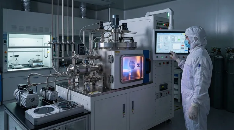
Mastering the CVD process requires equipment that delivers exceptional control and reliability. KINTEK's advanced high-temperature furnace solutions, including our specialized Tube and Vacuum & Atmosphere Furnaces, are engineered to provide the stable, high-purity environment essential for successful CVD.
Our strong in-house manufacturing and deep customization capabilities allow us to tailor a system to your exact experimental requirements, whether you are developing new semiconductor layers, hard ceramic coatings, or graphene films.
Let's build the future, one atomic layer at a time. Contact our experts today to discuss how we can support your thin film R&D.
Visual Guide
Related Products
- Custom Made Versatile CVD Tube Furnace Chemical Vapor Deposition CVD Equipment Machine
- MPCVD Machine System Reactor Bell-jar Resonator for Lab and Diamond Growth
- Multi Heating Zones CVD Tube Furnace Machine for Chemical Vapor Deposition Equipment
- 915MHz MPCVD Diamond Machine Microwave Plasma Chemical Vapor Deposition System Reactor
- Slide PECVD Tube Furnace with Liquid Gasifier PECVD Machine
People Also Ask
- How does CVD tube furnace sintering enhance graphene growth? Achieve Superior Crystallinity and High Electron Mobility
- What is a CVD tube furnace and what is its primary function? Discover Precision Thin-Film Deposition
- What temperature range do standard CVD tube furnaces operate at? Unlock Precision for Your Material Deposition
- What are the key application fields of CVD tube furnaces? Unlock Precision in Thin-Film Synthesis
- What are the benefits of developing new precursor materials for CVD tube furnaces? Unlock Advanced Thin-Film Synthesis


