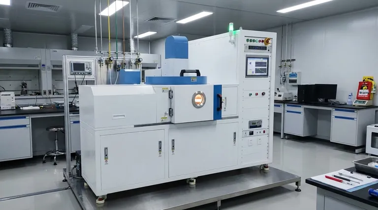
While highly versatile, Plasma-Enhanced Chemical Vapor Deposition (PECVD) is not a universally perfect solution. Its primary disadvantages stem from the complexity of managing a plasma environment, which can lead to challenges in process control, potential damage to the substrate surface from ion bombardment, and limitations in the physical properties of the deposited film compared to other methods.
PECVD exchanges the high-temperature requirement of conventional CVD for increased process complexity. Its main drawbacks are a direct consequence of using an energized plasma, creating trade-offs between processing temperature, film quality, and operational stability.
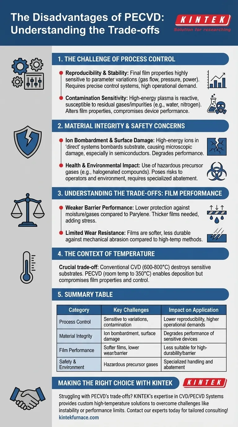
The Challenge of Process Control
The use of plasma introduces several variables that are inherently more difficult to manage than the purely thermal reactions of conventional CVD. This complexity is a primary source of PECVD's disadvantages.
Reproducibility and Stability
Maintaining stable and reproducible deposition conditions is a significant challenge. The final film's properties are highly sensitive to slight variations in parameters like gas flow rates, chamber pressure, RF power, and frequency.
Achieving identical results from run to run requires exceptionally precise control systems and meticulous process monitoring, making it more operationally demanding than simpler deposition techniques.
Contamination Sensitivity
The high-energy plasma environment is highly reactive and susceptible to contamination. Any residual gases or impurities within the deposition chamber, such as water vapor or nitrogen, can be incorporated into the film.
This can unintentionally alter the film’s chemical, optical, or electrical properties, compromising the final device's performance and reliability.
Material Integrity and Safety Concerns
The interaction between the plasma and the substrate is not always benign. The very mechanism that allows for low-temperature deposition can also introduce undesirable side effects.
Ion Bombardment and Surface Damage
In "direct" PECVD systems, the substrate is immersed in the plasma. This exposes its surface to bombardment by high-energy ions, which can create microscopic damage.
For sensitive applications like semiconductors, this damage can increase the electrical recombination rate near the surface, degrading device performance. This issue can be mitigated by using "remote" PECVD, where the plasma is generated away from the substrate, but this adds to system complexity.
Health and Environmental Impact
Certain PECVD processes use precursor gases that are hazardous or have a significant environmental impact. Halogenated compounds, for example, can pose health risks to operators and require specialized handling and abatement systems.
Understanding the Trade-offs: Film Performance
The advantages of PECVD's low deposition temperature often come with compromises in the final film's physical characteristics when compared to higher-temperature processes or alternative coating technologies.
Weaker Barrier Performance
PECVD films can offer lower barrier performance against moisture and gases compared to coatings like Parylene. Achieving high-integrity protection may require depositing a thicker film, which can add stress and impact device geometry.
Limited Wear Resistance
The films produced by PECVD are often softer and exhibit lower wear resistance than films deposited using higher-temperature methods. This makes them less suitable for applications requiring a durable exterior surface exposed to mechanical abrasion.
The Context of Temperature
It is critical to remember that these trade-offs exist for a reason. Conventional CVD requires temperatures of 600-800°C, which would destroy or damage temperature-sensitive substrates like polymers, plastics, and many electronic components.
PECVD’s ability to operate from room temperature to around 350°C is its defining advantage. The disadvantages in film properties and process control are the price paid to enable deposition on these delicate materials.
Making the Right Choice for Your Application
Choosing a deposition method requires aligning its capabilities and drawbacks with your primary goal.
- If your primary focus is depositing on temperature-sensitive substrates: PECVD is often the superior or only viable choice, and its process complexities must be managed.
- If your primary focus is maximum wear resistance or barrier performance: You should evaluate if the substrate can tolerate higher-temperature CVD or consider alternative technologies like PVD or ALD.
- If your primary focus is process simplicity and cost for a heat-tolerant substrate: Conventional thermal CVD may provide a more robust and less complex solution.
Ultimately, selecting PECVD is a conscious engineering decision to trade process simplicity for the critical advantage of low-temperature film deposition.
Summary Table:
| Disadvantage Category | Key Challenges | Impact on Application |
|---|---|---|
| Process Control | Sensitive to parameter variations, contamination risk | Lower reproducibility, higher operational demands |
| Material Integrity | Ion bombardment can cause surface damage | Degrades performance of sensitive electronic devices |
| Film Performance | Softer films, lower wear/barrier performance vs. high-temp CVD | Less suitable for high-durability or high-barrier applications |
| Safety & Environment | Use of hazardous precursor gases | Requires specialized handling and abatement systems |
Struggling with PECVD's trade-offs for your specific materials? KINTEK's expertise is your solution. We leverage exceptional R&D and in-house manufacturing to provide advanced high-temperature furnace solutions, including our specialized CVD/PECVD Systems. Our strong deep customization capability allows us to tailor systems—whether Muffle, Tube, Rotary, Vacuum & Atmosphere, or CVD/PECVD—to precisely overcome challenges like process instability or film performance limitations. Let us help you optimize your deposition process. Contact our experts today for a consultation tailored to your unique experimental requirements!
Visual Guide
Related Products
- Slide PECVD Tube Furnace with Liquid Gasifier PECVD Machine
- RF PECVD System Radio Frequency Plasma Enhanced Chemical Vapor Deposition
- Inclined Rotary Plasma Enhanced Chemical Deposition PECVD Tube Furnace Machine
- Inclined Rotary Plasma Enhanced Chemical Deposition PECVD Tube Furnace Machine
- Multi Heating Zones CVD Tube Furnace Machine for Chemical Vapor Deposition Equipment
People Also Ask
- What plasma source is used in PE-CVD tube furnaces? Unlock Low-Temperature, High-Quality Deposition
- What are the main advantages of PECVD tube furnaces compared to CVD tube furnaces? Lower Temp, Faster Deposition, and More
- What are the disadvantages of tube furnace cracking when processing heavy raw materials? Avoid Costly Downtime and Inefficiency
- What are the advantages of using a tube furnace CVD system for Cu(111)/graphene? Superior Scalability and Quality
- What is plasma in the context of PECVD? Unlock Low-Temperature Thin Film Deposition


