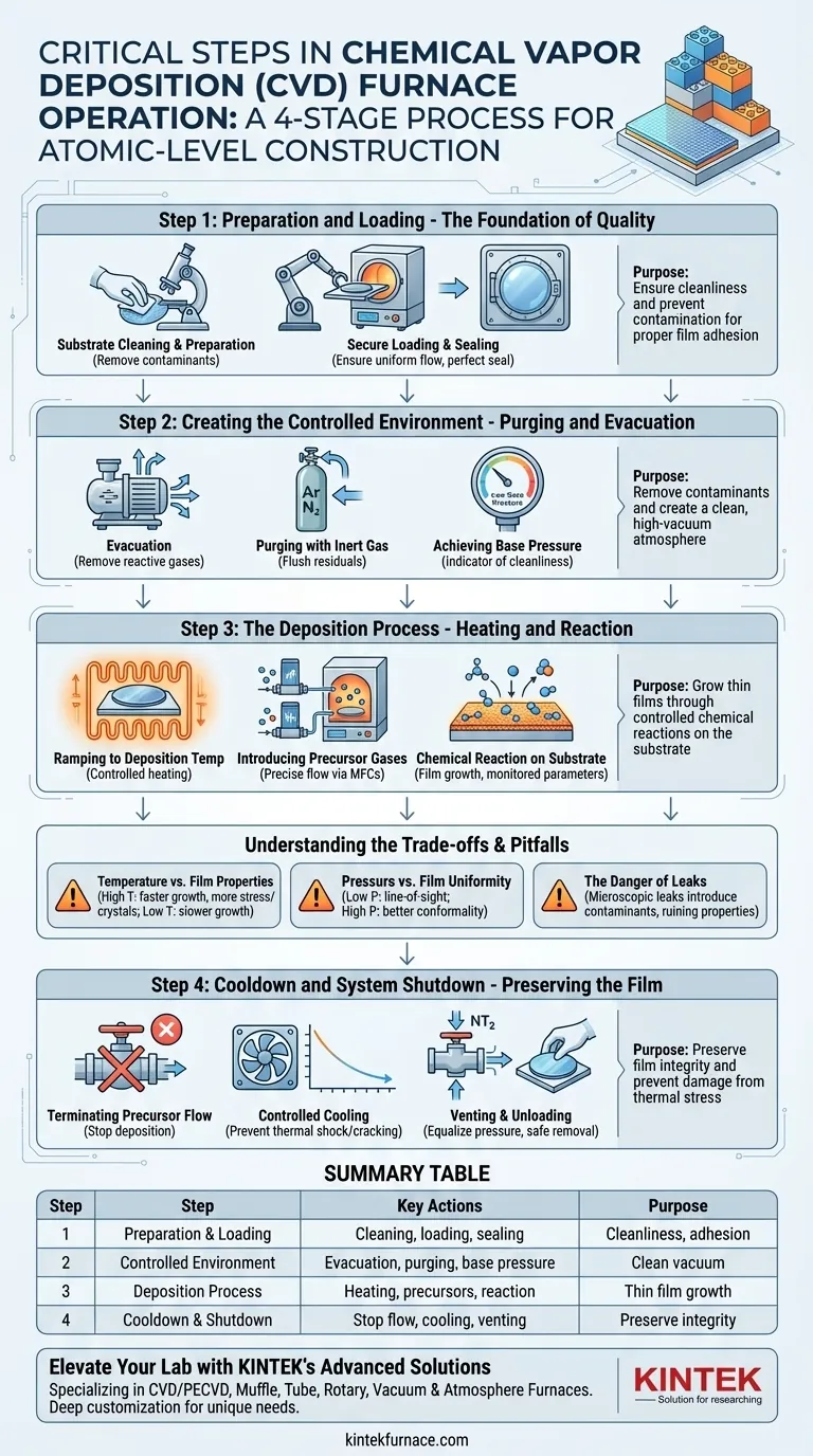
At its core, operating a chemical vapor deposition (CVD) furnace is a four-stage process designed for atomic-level construction. It begins with preparing the chamber and substrate, then creating a highly controlled, ultra-clean environment. This is followed by the actual deposition, where heat and precursor gases react to grow a thin film, and concludes with a careful cooldown and shutdown to preserve the newly created material.
The success of chemical vapor deposition hinges less on the chemical reaction itself and more on the meticulous control of the environment—vacuum, temperature, and gas flow—at every stage. A failure in preparation or control at any step will directly compromise the quality and integrity of the final thin film.

Step 1: Preparation and Loading - The Foundation of Quality
This initial phase is about setting the stage for a successful deposition. Any oversight here will invariably lead to defects in the final film.
Substrate Cleaning and Preparation
Before anything else, the substrate—the material upon which the film will be grown—must be impeccably clean. Any microscopic dust, oils, or oxides will act as a barrier or a point of contamination, preventing proper film adhesion and creating defects.
This often involves a multi-step chemical cleaning process, followed by careful handling in a clean environment to prevent re-contamination before it enters the furnace.
Secure Loading and Sealing
The clean substrate is carefully loaded into the furnace chamber. Its position and orientation are critical for ensuring the uniform flow of gases across its surface, which directly impacts the uniformity of the deposited film.
Once loaded, the furnace door must be sealed perfectly. A proper seal is essential for achieving the high vacuum required for the process and preventing atmospheric contaminants from leaking into the chamber during operation.
Step 2: Creating the Controlled Environment - Purging and Evacuation
With the substrate inside, the next goal is to remove the ambient air and replace it with a precisely managed atmosphere.
The Role of the Vacuum System
The process begins by evacuating the chamber using a series of vacuum pumps. A mechanical or "roughing" pump first removes the bulk of the air. Then, a high-vacuum pump, like a turbomolecular or diffusion pump, takes over to achieve a much lower pressure.
The purpose is to remove reactive gases like oxygen and water vapor, which would interfere with the desired chemical reaction and contaminate the film.
Purging with Inert Gas
To further flush out residual contaminants, the chamber is often "purged" by backfilling it with a high-purity inert gas, such as argon (Ar) or nitrogen (N₂), and then evacuating it again. This cycle may be repeated several times.
Achieving Base Pressure
The system is pumped down to its "base pressure," the lowest possible pressure before introducing the process gases. This pressure is a key indicator of the chamber's cleanliness and seal integrity. A good, low base pressure is a prerequisite for high-quality film growth.
Step 3: The Deposition Process - Heating and Reaction
This is the active phase where the thin film is actually constructed, molecule by molecule.
Ramping to Deposition Temperature
The furnace begins heating the substrate to the target deposition temperature. This is done via a controlled "ramp" to prevent thermal shock, which could crack the substrate or other furnace components.
Introducing Precursor Gases
Once at temperature, the precursor gases are introduced into the chamber. These are the gaseous "building blocks" of the film. Their flow rates are controlled with extreme precision by Mass Flow Controllers (MFCs).
The pressure inside the chamber is carefully regulated during this step, as it influences how the gas molecules travel and react.
The Chemical Reaction on the Substrate
The high temperature provides the energy for the precursor gases to react or decompose on the hot substrate surface, forming a solid, stable thin film. This process can last from minutes to many hours, depending on the desired film thickness. Throughout this time, all parameters—temperature, pressure, and gas flows—are monitored continuously.
Understanding the Trade-offs and Pitfalls
Achieving a perfect film requires balancing competing factors and avoiding common failures.
Temperature vs. Film Properties
Higher temperatures often increase the deposition rate but can also lead to higher stress in the film or unwanted crystalline structures. The optimal temperature is a trade-off between growth speed and desired material properties.
Pressure vs. Film Uniformity
Chamber pressure affects the "mean free path" of gas molecules. At lower pressures, molecules travel in straighter lines, which can lead to "line-of-sight" coating. At higher pressures, more gas-phase collisions occur, which can improve how uniformly the film coats complex shapes.
The Danger of Leaks
Even a microscopic leak in the vacuum system is a critical failure. It will continuously introduce contaminants like oxygen and water, which can become incorporated into the film, ruining its electrical, optical, or mechanical properties. Constant monitoring of the chamber pressure is essential to detect leaks.
Step 4: Cooldown and System Shutdown - Preserving the Film
The final steps are just as critical as the first; improper shutdown can destroy the work that was just completed.
Terminating Precursor Flow
The first action is to shut off the flow of the reactive precursor gases, immediately stopping the deposition process. The flow of inert gas is often maintained during the initial cooldown.
Controlled Cooling
The furnace is then cooled down in a controlled manner. Cooling too quickly can induce thermal stress, causing the newly formed film to crack or delaminate from the substrate.
Venting and Unloading
Once the furnace has cooled to a safe temperature (typically near room temperature), the chamber must be brought back to atmospheric pressure. This is done by "venting" or backfilling the chamber with an inert gas like nitrogen.
Only after the chamber pressure is equalized with the outside atmosphere can the door be safely opened and the finished substrate be removed.
Making the Right Choice for Your Process
Your operational focus will depend on the specific goal of your deposition run.
- If your primary focus is film quality and purity: Concentrate on meticulous substrate cleaning and achieving the lowest possible base pressure before deposition begins.
- If your primary focus is process repeatability: Document every single parameter, including pump-down times, base pressure, temperature ramps, gas flow rates, and cooldown profiles for every run.
- If your primary focus is safety and equipment longevity: Always follow proper vacuum procedures, use controlled heating and cooling ramps, and never attempt to open a chamber that is under vacuum or hot.
Mastering this sequence of precise environmental controls transforms the CVD process from an art into a predictable and powerful manufacturing science.
Summary Table:
| Step | Key Actions | Purpose |
|---|---|---|
| 1. Preparation and Loading | Substrate cleaning, secure loading, sealing | Ensure cleanliness and prevent contamination for proper film adhesion |
| 2. Controlled Environment | Evacuation, purging with inert gas, achieving base pressure | Remove contaminants and create a clean, high-vacuum atmosphere |
| 3. Deposition Process | Heating to temperature, introducing precursor gases, monitoring reactions | Grow thin films through controlled chemical reactions on the substrate |
| 4. Cooldown and Shutdown | Terminating gas flow, controlled cooling, venting, and unloading | Preserve film integrity and prevent damage from thermal stress |
Ready to elevate your laboratory's capabilities with advanced high-temperature furnace solutions? KINTEK specializes in providing diverse labs with cutting-edge equipment like CVD/PECVD Systems, Muffle, Tube, Rotary, Vacuum & Atmosphere Furnaces. Leveraging our exceptional R&D and in-house manufacturing, we offer strong deep customization to precisely meet your unique experimental needs. Contact us today to discuss how our tailored solutions can enhance your process efficiency and film quality!
Visual Guide
Related Products
- Custom Made Versatile CVD Tube Furnace Chemical Vapor Deposition CVD Equipment Machine
- Slide PECVD Tube Furnace with Liquid Gasifier PECVD Machine
- Multi Heating Zones CVD Tube Furnace Machine for Chemical Vapor Deposition Equipment
- MPCVD Machine System Reactor Bell-jar Resonator for Lab and Diamond Growth
- RF PECVD System Radio Frequency Plasma Enhanced Chemical Vapor Deposition
People Also Ask
- What is a CVD tube furnace and what is its primary function? Discover Precision Thin-Film Deposition
- What are the key application fields of CVD tube furnaces? Unlock Precision in Thin-Film Synthesis
- What customization options are available for CVD tube furnaces? Tailor Your System for Superior Material Synthesis
- How might AI and machine learning enhance CVD tube furnace processes? Boost Quality, Speed, and Safety
- What improvements can be made to the bonding force of gate dielectric films using a CVD tube furnace? Enhance Adhesion for Reliable Devices


