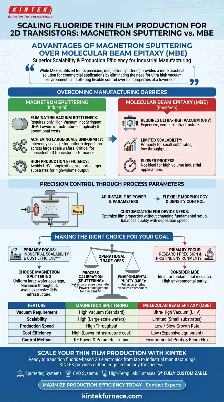
Magnetron sputtering distinguishes itself through superior scalability and production efficiency compared to molecular beam epitaxy (MBE). It enables the uniform deposition of fluoride thin films across large-scale wafers, making it the preferred choice for industrial manufacturing where throughput is critical.
While MBE is utilized for its precision, magnetron sputtering provides a more practical solution for commercial applications by eliminating the need for ultra-high vacuum environments and offering flexible control over film properties at a lower cost.
Overcoming Manufacturing Barriers
Eliminating the Vacuum Bottleneck
One of the most significant advantages of magnetron sputtering is that it does not require the stringent ultra-high vacuum (UHV) conditions essential for MBE.
This relaxes the complexity of the equipment infrastructure required for fabrication. Consequently, it lowers the barrier to entry for manufacturing and directly reduces operational costs.
Achieving Large-Scale Uniformity
Sputtering is inherently designed for process scalability, a vital requirement for transition from research to production.
The technique ensures uniform film deposition across large-scale wafers, which is critical for maintaining consistent performance across millions of 2D transistors.
High Production Efficiency
Because it avoids the complexities of UHV and supports larger substrates, magnetron sputtering offers higher production efficiency.
This makes it a more viable candidate for high-volume industrial applications compared to the slower, more restrictive MBE process.
Precision Control Through Process Parameters
Flexible Morphology Tuning
Magnetron sputtering allows for direct manipulation of the film's physical characteristics.
By adjusting radio frequency (RF) power and other process parameters, engineers can flexibly control the morphology and density of the fluoride films.
Customization for Device Needs
This tunability ensures that the film's properties can be optimized for specific transistor requirements without changing the fundamental equipment setup.
It provides a method to balance film quality with deposition speed, adapting to the specific needs of the 2D transistor architecture.
Understanding the Operational Trade-offs
Process Calibration vs. Environment
While sputtering removes the need for a UHV environment, it shifts the burden of quality control to parameter management.
Achieving the correct film density requires precise calibration of the RF power. Unlike MBE, which relies on a pristine vacuum environment for purity, sputtering relies on the kinetic control of the deposition process to achieve the desired film structure.
Making the Right Choice for Your Goal
When selecting a deposition method for fluoride thin films in 2D transistors, consider your project's scale and resources.
- If your primary focus is industrial scalability: Choose magnetron sputtering to ensure uniform coverage across large wafers and maximize production throughput.
- If your primary focus is cost efficiency: Leverage sputtering to avoid the expensive infrastructure associated with the ultra-high vacuum requirements of MBE.
By prioritizing scalability and flexible control, magnetron sputtering provides a robust pathway for transitioning fluoride-based 2D electronics from the lab to the production line.
Summary Table:
| Feature | Magnetron Sputtering | Molecular Beam Epitaxy (MBE) |
|---|---|---|
| Vacuum Requirement | High Vacuum (Standard) | Ultra-High Vacuum (UHV) |
| Scalability | High (Large-scale wafers) | Limited (Small substrates) |
| Production Speed | High Throughput | Low / Slow Growth Rate |
| Cost Efficiency | High (Lower infrastructure cost) | Low (Expensive equipment) |
| Control Method | RF Power & Parameter Tuning | Environmental Purity & Beam Flux |
Scale Your Thin Film Production with KINTEK
Ready to transition your fluoride-based 2D electronics from lab research to industrial-scale manufacturing? KINTEK provides the cutting-edge technology you need to succeed.
Backed by expert R&D and precision manufacturing, we offer a comprehensive range of Sputtering Systems, CVD systems, and high-temp lab furnaces—all fully customizable to meet your unique thin-film architecture requirements. Our equipment empowers you to achieve superior film uniformity and density without the prohibitive costs of UHV infrastructure.
Maximize your production efficiency today. Contact our technical experts to find the perfect customized solution for your 2D transistor fabrication needs.
Visual Guide
References
- Thin Fluoride Insulators for Improved 2D Transistors: From Deposition Methods to Recent Applications. DOI: 10.1002/pssr.202500200
This article is also based on technical information from Kintek Furnace Knowledge Base .
Related Products
- 915MHz MPCVD Diamond Machine Microwave Plasma Chemical Vapor Deposition System Reactor
- Multi Heating Zones CVD Tube Furnace Machine for Chemical Vapor Deposition Equipment
- Cylindrical Resonator MPCVD Machine System for Lab Diamond Growth
- Slide PECVD Tube Furnace with Liquid Gasifier PECVD Machine
- Custom Made Versatile CVD Tube Furnace Chemical Vapor Deposition CVD Equipment Machine
People Also Ask
- What are the essential components of an MPCVD reactor for diamond film deposition? Unlock High-Quality Diamond Growth
- In which industries is the microwave plasma chemical vapor deposition system commonly used? Unlock High-Purity Material Synthesis
- What are the essential components of an MPCVD reactor system? Build a Pristine Environment for High-Purity Materials
- What is the purpose of a microwave plasma chemical vapor deposition system? Grow High-Purity Diamonds and Advanced Materials
- What is the basic principle of operation for the microwave plasma chemical vapor deposition system? Unlock High-Purity Material Growth


